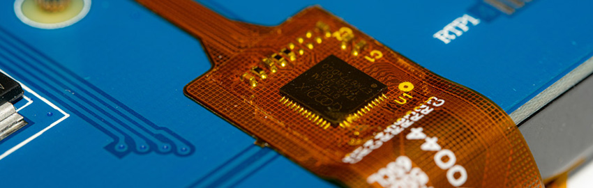
If manufacturers understood the true value and opportunity of their excess and obsolete (E&O) electronic component stock, they would take a much more proactive approach to ensure this surplus inventory is not written off and sent to landfill.
In reality, E&O inventory is not an operational inconvenience but a financial opportunity and sustainable responsibility. Provided E&O stock is brand new, unused and in the original manufacturer’s packaging, manufacturers can likely redistribute the parts on the secondary market to another manufacturer for use. This not only recoups value for the redistributing company, but also promotes a circular economy, extending the lifetime value of the materials inside.
Are you consistently solving problems and adding value?
For an organization to improve, its culture must embrace change. Determining and measuring organizational culture presents challenges since it can often be ambiguous and difficult to quantify. Organizational culture is a shared belief system consisting of an organization’s philosophy, traditions, shared expectations, work ethics and values that hold it together.
Six steps for limiting interference and data loss.
Printed circuit boards (PCBs) utilizing Bluetooth technology can encounter issues like interference, lost data and poor signal integrity if certain precautions aren't taken. This guide outlines essential rules and guidelines for selecting Bluetooth technology for various applications and, more specifically, for integrating it into circuit boards.
A variety of applications utilize Bluetooth, including:
Beacons used in shopping malls
Eddystone frames for industrial sensing applications
Headsets and audio/stereo products
Remote peripheral devices such as video game controllers or computer mice/keyboards
Home automation systems
Wireless consumer electronics applications, including cameras, printers and phones.
Each application incorporates the same common Bluetooth technology but adapts it based on connection types. Design engineers must apply fundamental principles to optimize signal integrity and enhance overall device effectiveness.
While Bluetooth is not as fast a wireless choice compared to Wi-Fi, it is getting faster. Its performance declines when obstructed by walls or nearby objects, and range is limited.
Despite these challenges, Bluetooth remains a strong choice. The latest version, 5.0, shows significant improvements over 4.2. Overall, Bluetooth provides a low-power, reliable and secure solution that integrates easily into a range of small peripherals.
Bluetooth has been around for more than 20 years and is still evolving, and although it’s improved in speed, power, range, security and other attributes over the years, some of the issues seen at its conception in the mid-90s remain, including its susceptibility to signal interference.
So, what can be done from a PCB design standpoint to optimize signal integrity, minimize interference and lost data packets?
Here are a few Bluetooth circuit design considerations and general rules of thumb:
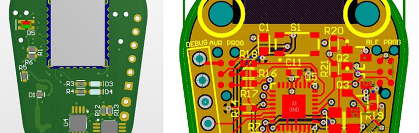
Use certified modules. When incorporating Bluetooth into a product with limited resources, consider a pre-certified, fully contained module to accelerate development and reduce time-to-market. While this choice may slightly increase costs, it often prevents headaches related to antenna placement, design issues and EMI susceptibility. Many reasonably priced certified modules are available today, typically featuring a small ARM processor such as the RN4020 or RN4870 from Microchip or the BT121 or BGM113 from Silicon Labs. The on-board processor provides greater flexibility and power, allowing control of simple peripherals through GPIO, SPI, I2C, PWM and more, in addition to managing the Bluetooth stack.
Figure 1.Sample Bluetooth boards.
Check the Bluetooth device selection. Ensure an appropriate Bluetooth device is chosen for the application and the antenna is appropriately sized and tuned.
For a simple beacon application requiring short bursts of location or data advertising, opt for a low-power device using Bluetooth Low Energy (BLE). This cost-effective solution minimizes features and peripherals, helping to save on-board space and reduce overall costs (Figure 2).
Figure 2.For simple beacon applications, a low-power BLE is a cost-effective solution and can save board real estate.
If a higher throughput, audio-streaming or data-exchanging Bluetooth application is needed, select a device with increased transmit (Tx) power, higher receiver (Rx) sensitivity and a faster data-rate (although slowing the data rate can typically help with minimizing dropped packets).
Need an all-in-one chip? Consider chipsets containing powerful or secondary processors with available UART, SPI, I2C, PWM, ADC, DAC and GPIO pins. If the project relies heavily on received signal strength indicator (RSSI) readings, ensure the device provides adequate decibel (dB) resolution on its RSSI monitor.
Separate or remove copper signals and high-energy components. When designing in a Bluetooth chipset or module, keep the antenna completely free from nearby copper signals or components carrying significant amounts of energy (especially switched power paths, such as boost or buck converters).
This includes keeping the area (and board layers) free of planes and polygon pours. Most Bluetooth chipset manufacturers will provide layout guidelines to follow closely during PCB design. When manually laying out the antenna area, use a ground plane as appropriate to keep a good bandwidth at the input and make sure to build in room for tuning elements (a ground plane is required for printed and ceramic antennas).
Ground stitching vias prevent unwanted radiation from the PCB edge which could otherwise penetrate nearby Bluetooth signals. When possible, optimize the board shape to the Bluetooth device’s antenna location, keeping it on the edge and far away from nearby components and signals. If using analog-based signals such as audio, separate analog and digital ground planes.
And it’s always a good idea to shield the electronics (not the antenna, of course) to prevent cross-coupling and minimize picked up noise.
Consult power supply notes. Ensure the rail supplying power to the Bluetooth module or chip is clean. Use bypass capacitors (1.0µF) and decoupling capacitors (0.1µF and 10nF) where needed. Additionally, incorporate ferrite beads on the power rail entering the Bluetooth area of the board to effectively reject high-frequency noise.
Tools and analysis. If designing the antenna area, make sure have the proper equipment (such as a network analyzer) is available to analyze and tune the matching network, or consider sending the design to a third-party RF test lab.
Consider real-world obstructions. A wide variety of things can cause obstruction or de-tuning during a Bluetooth connection, including nearby water (humans too … we’re made mostly of water), metallized objects, smartphones/tablets, computers, devices operating on the same ISM band (such as microwave ovens or WLAN technologies), power sources, wireless RF video, office lighting and home phones.
The device is highly susceptible to signal loss, even at distances of just 1-2 meters. If there is a higher risk of these kinds of things impacting signal quality, choose a higher power device and operate at a slower speed to minimize packet drop. When electronics are housed in an enclosure, ensure that metallized materials are minimized and positioned far away from the BLE module. The relationship between Bluetooth signal strength and distance is nonlinear and somewhat unpredictable based on the surrounding environment, though it generally follows the pattern shown in Figure 3.
Figure 3.A graph showing the relationship between Bluetooth signal strength and distance.
Whether designing a small, simple Beacon module or a data-streaming, power-hungry Bluetooth hub, following these considerations could save tons of headaches during the test/implementation stage of design.
With the expansion of Bluetooth PCB assembly, it’s an exciting time to incorporate wireless communication and control into products, and the future will only bring smaller, faster, cheaper and stronger Bluetooth components.
Andrew Gonzales is VP of engineering at San Francisco Circuits (sfcircuits.com); This email address is being protected from spambots. You need JavaScript enabled to view it.. Jason Metzner is a senior systems engineer at Arthrex (arthrex.com).
A summary of how to order layers to achieve target impedance values.
Printed circuit boards are becoming highly dense, hosting all kinds of high-speed interfaces. The bandwidth of the clock frequencies reaches hundreds of GHz, leading to complex issues related to EMI interference, crosstalk, reflections, jitter and losses.
These new challenges impact all processes involved in design, analysis, manufacturing and testing. Manufacturers employ advanced and complex technologies and methods to accommodate the higher density of functionalities packed into smaller components. To manage losses and achieve desired functionality at higher speeds, research into new materials is leading and revolutionizing this industry. The PCB is at the center of issues related to signal integrity, power integrity, electromagnetic interference, crosstalk, mechanical, thermal and more. It also plays an integral role in solutions for each of these challenges.
These issues begin at PCB stack-up design, since a well-designed stack-up forms the foundation of a strong and stable PCB. It acts as the fundamental backbone of the PCB design structure that impacts signal integrity, power distribution and signal impedance. A sound and properly designed stack-up minimizes the circuit’s vulnerability to external noise and helps improve the electromagnetic compatibility of the product (Figure 1).
Figure 1.The PCB is the center of a host of electrical, mechanical and thermal issues.
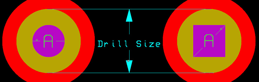
What follows is a summary of some key SI-related points in simple terms, without delving into deep mathematical calculations and complex theories. The stack-up is the arrangement of conductive and insulating layers within a PCB. The total number of layers in a stack-up is determined by the higher pin count ball grid array (BGA) components, complexity of the circuit, its placement and performance requirements. The order of these layers is very important and should be finalized carefully, taking into consideration manufacturability requirements and signal integrity (Figure 2).
Figure 2.Sample PCB stack-up configuration.
Regarding insulating layers, pay special attention to the properties of the dielectric material and its width. The type of material and its thickness significantly impact signal speed, impedance and losses. These materials play an important role in managing the mechanical and thermal stresses in the PCB, while the width of the dielectric material also contributes to the overall PCB width. Some conductive layers serve as power or ground planes (power/GND), while others function as dedicated signal layers. Designers use plane layers to establish power delivery networks (PDN) and carry high power signals from the power supply to their respective loads. In contrast, signal layers connect all manner of critical high-speed and other general inter-IC connections. Critical signals, which include high-speed signals on a PCB, require special attention and are highlighted in IC vendor datasheets.
Designers cannot route these signals on just any layer; they must meet specific timing and impedance-based requirements for the product to function correctly. For example, consider memory, the bread and butter of every design. DDR3 memory, for instance, operates as a high-speed interface that contains all types of signals, including data, strobes, address, command, control, status and clock signals. This interface can feature over 100 signals, each with specific timing and impedance requirements (Figures 3 and 4). The strobe and clock signals are differential in nature, while the remainder are single-ended, with different impedance requirements.
Figure 3.50Ω single-ended signal routing in DDR3 interfaces.
Figure 4.100Ω differential pair routing for DDR3 clock and strobe signals.
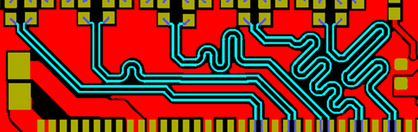
Regarding timing-related constraints, at a high level, data bits exist as bytes/lanes and each lane has its own differential strobe. In each lane, every data bit must maintain a timing relationship with its strobe and match the length of the strobes within a certain tolerance as provided in the datasheet. Additionally, all these data lanes must maintain a specific timing among themselves. All strobes in all lanes must maintain their timing with respect to the clock. The clock requires all address/command/control signals to match its length as well (Figure 5).
Figure 5.Serpentine routing for length-matching of DDR3 data, strobe and clock signals.
Design engineers mention these delay requirements in terms of time units, such as picoseconds or nanoseconds, while PCB layout designers prefer length-based constraints such as millimeters or mils. Converting time into distance depends on the signal’s speed on that particular layer, which relies on the properties of the dielectric material around the signal trace. These material properties also impact the trace impedance. All these factors are a part of PCB stack-up design, linking both speed and impedance closely to this design process. Let's explore how this connection works.
Stack-up design → Signal speeds
When electrical signals travel on the PCB traces, they generate waves of electromagnetic fields around them that travel along with the signals. These electromagnetic (EM) waves travel through the materials surrounding the PCB trace. In free space, EM waves propagate at the speed of light, which is 3x10^8m/s. In a PCB, however, there is no free space; instead, dielectric materials surround the signal traces. The speed of the EM fields in a PCB is affected by the effective relative permittivity (Er) value of the insulating material and is therefore equal to the speed of light in a vacuum, divided by the square root of the effective Er value of the insulating materials surrounding the transmission line; i.e.,
v = c / sqrt(Er)
In PCBs, FR-4 is the common dielectric material used, and its dielectric constant has a range of values from 3.9 to 4.7. To make it simple, take Er = 4 and put it in the above equation, which then reduces to
v = c / sqrt (4) = c / 2 = 1.5 x 10^8m/s = 150mm/ns ~ 6in/ns
In a PCB, the signal trace exists on an external layer (TOP/BOTTOM) or on an internal layer. When the signal trace resides on an internal layer, with a reference plane above and below it, as shown in Figure 6, the configuration is called a stripline configuration.
Figure 6.Offset stripline 1B1A configuration with signal trace between two reference planes.
In this configuration, the trace is completely surrounded by the dielectric material. Thus, the effective dielectric constant for this trace is equal to the Er value of the insulating material. For an Er value of 4, the speed of the signal on the internal layer will be approximately 6in/ns. The configuration in which a Cu trace is present on an external layer with a reference plane under it is called microstrip line configuration (Figure 7). In this configuration, the trace has dielectric material below it while air and solder mask typically sit above it. The Er value of the air/solder mask is less than that of FR-4. As a result, the effective Er value for the microstrip line drops below 4, leadings to higher signal speeds on external layers, meaning v > 6 in/ns. Signals always travel faster on external layers. Therefore, a signal routed on an external layer with a certain length experiences less delay compared to the same length of signal routed on the internal layer. Traces of the same length routed on different layers may have different delay times depending on the effective Er value for each respective layer.
Figure 7.Surface microstrip 1B configuration with a copper trace on the external layer.
From the SI timing point of view, this point is crucial when routing signals in an interface that needs to be length-matched. Route signals belonging to the same group on the same layer to control and easily match the delays. This practice explains why all signals of a DDR3 byte lane are routed on the same layer: it ensures they all maintain the same speed and, consequently, the same delay. Modern day layout tools have this capability built in. If the PCB stack-up is defined properly and all details of material properties and their widths provided, the tool calculates the signal speeds on every layer and can convert the delays into lengths (Figure 8).
Figure 8.Routing byte lane signals on the same layer.
Stack-up design → Trace impedance, Zo
Now it is time to discuss the relation of characteristic impedance, Zo, with the stack-up design. Closely review the Cu trace in the PCB: it makes a parallel plate capacitor with the reference plane below (Figures 9 and 10).
Figure 9.Copper trace and reference plane form a parallel plate capacitor.
Figure 10.Surface microstrip configuration (1B) affects impedance and signal integrity.
In a parallel plate capacitor, the two plates are separated from one another by air or by a dielectric material in the same way the trace is separated from the plane by an insulating material.
The capacitance of the capacitor is linked to the overlapping area of the plates (A), the distance between the two plates (d) and dielectric constant (Er) of the insulating material between the plates, through this formula
Capacitance = (A x Er) / d
For the capacitance of the PCB trace, the above formula can be written as
C = (w x Er) / h
The trace impedance, Zo, and its capacitance are related by the formula
Zo = sqrt (L/C)
It is evident and can be easily concluded that the trace impedance, Zo, is inversely related to its capacitance, C; i.e.,
Zo ⇐ ⇒ 1/C
This means that the factors that will increase the trace capacitance will in turn decrease its impedance, and vice versa. Keeping in view the formula C = (w x Er)/h, it can be concluded that:
Increasing trace width, w, will increase trace capacitance but will decrease the trace impedance, Zo, and vice versa.
Using insulating material with higher dielectric constant value (Er) will increase the trace capacitance, but will decrease its Zo and vice versa.
Increasing dielectric material thickness (h) will decrease the trace capacitance, but will increase its impedance, Zo, and vice versa.
So, in a nutshell:
Trace capacitance (C)
⇐ ⇒
Trace impedance (Zo)
C → w
⇐ ⇒
Zo → 1/w
C → Er
⇐ ⇒
Zo → 1/Er
C → 1/h
⇐ ⇒
Zo → h
The trace impedance inversely relates to its width (w) and the dielectric constant value (Er) of the dielectric material, while it directly relates to the thickness of the dielectric material. These factors directly connect to the PCB stack-up. These parameters are tweaked to find suitable trace widths that achieve different target impedance values for all SE and diff-pairs. While making these calculations, ensure that the specified trace widths and spacing values are manufacturable and that selected materials are economical. Additionally, ensure impedance targets are met while keeping the thickness of the dielectric materials so that the overall PCB thickness is within allowable specs.
The stack-up design directly impacts signal speeds and trace impedances through the selected material properties in PCB layer construction. Engineers calculate and control parameters that affect multiple things at once. For example, changing the value of Er impacts both the trace impedance Zo and the signal speed. Sometimes, engineers alter material properties simply to achieve target impedance values, ignoring their impact on signal speeds. The result can be timing issues – product failure.
Akber Roy is chief executive of Rush PCB (rushpcb.com), a printed circuit design, fabrication and assembly company; This email address is being protected from spambots. You need JavaScript enabled to view it..