A manufacturer’s perspective on determining parts layout.
A land pattern refers to the footprint or layout of surface-mount components on a printed circuit board (PCB). It includes the arrangement of pads, or lands, to which component leads or terminals will be soldered. An accurate land pattern is crucial for ensuring reliable solder joints, proper alignment of components and optimal electrical performance of the circuit. Most electronic component manufacturers provide detailed specifications and guidelines for creating land patterns specific to each component, which should be followed closely during PCB design.
Key aspects of a component land pattern include the following:
- Pad layout: The shape, size and spacing of pads where the component leads will be soldered.
- Dimensions: Exact dimensions of each pad, including width, length and pitch (distance between pads).
- Keep-out areas: Areas on the PCB where no traces or components should be placed to avoid interference or damage.
- Solder mask: The solder mask defines where solder should and should not adhere, ensuring proper connections and preventing solder bridges.
- Silkscreen: Markings on the PCB indicating component placement, orientation and other important information.
Component Mounting
Components are generally classified into two main types based on their installation method: through-hole components and surface-mount components (SMDs). Here’s a breakdown of each:
- Through-Hole Components:
- Passives (resistors, capacitors and diodes, etc.). These components have leads (pins) that are inserted through holes drilled in the PCB. The leads are then soldered to pads on the opposite side of the board.
- Actives (ICs). Active components such as ICs may also be mounted this way, with their leads inserted through the PCB and soldered on the other side.
Through-hole components are generally larger and can handle higher currents than surface-mount components. They are often used in applications where durability and reliability are critical, such as in industrial equipment and automotive electronics, and legacy products where a redesign is not feasible.
- Surface mount technology devices (SMDs):
- Passives (resistors, capacitors and diodes). These components have small, flat contacts (pads) on the bottom that adhere directly to pads on the PCB surface. They are soldered using a reflow soldering process, which involves applying solder paste to the pads, placing the components and heating the entire assembly to melt the solder.
- IC packages come in various sizes and shapes, often with leads terminating from the sides (such as QFP or SOIC) or below the package (e.g., BGA), and are mounted directly onto the PCB surface.
Surface mount components are generally smaller than through-hole (PTH) devices and have greater component density on PCBs. They are used widely in consumer electronics, mobile devices and compact electronics products where size and weight reduction are important factors.
Land Pattern Calculation
Pad size. For plated through-hole parts, the component pad size is determined using the following formulas (Figure 1):
- Minimum component PTH pad size = finished hole size + 0.016” (0.406mm)
- Preferred component PTH pad size = finished hole size + 0.021” (0.5334mm)
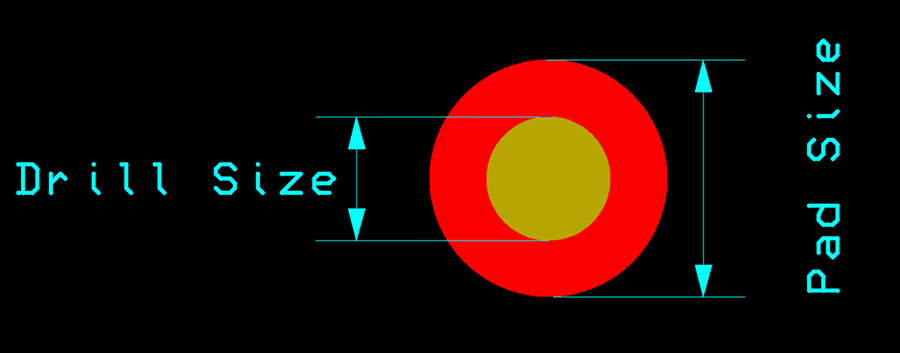
Figure 1. Hole size pad size.
Hole size. Hole size requirements for tin-lead wave-soldered PTH component pins are as follows (Figure 2):
- Minimum FHS = maximum lead diameter (Dimension A) + 0.012” (0.3048mm).
- Maximum FHS = maximum lead diameter (Dimension A) + 0.028” (0.7112mm).
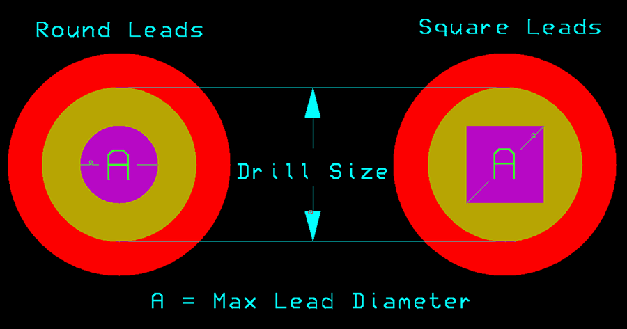
Figure 2. Hole size requirements for through-hole components.
We categorize the hole size requirements for lead-free wave-soldered through-hole component pins in the following two types:
Low thermal pass pins.
- Minimum FHS = maximum lead diameter (Dimension A) + 0.022” (0.5588mm)
- Maximum FHS = maximum lead diameter (Dimension A) + 0.026” (0.6604mm)
High thermal pass – adjacent pins.
- Minimum FHS = maximum lead diameter (Dimension A) + 0.028” (0.7112mm)
- Maximum FHS = maximum lead diameter (Dimension A) + 0.032” (0.8128mm)
High thermal pass – isolated pins.
- Minimum FHS = maximum lead diameter (Dimension A) + 0.038” (0.9652mm)
- Maximum FHS = maximum lead diameter (Dimension A) + 0.042” (1.0668mm)
For components with a pitch <0.100" (2.54mm), the hole diameter may have to be smaller than specified to avoid violating other design relationships. We recommend making these holes as large as possible up to the maximum size.
Table 1 and Figure 3 shows package sizes and sample land pattern dimensions for SMT passives ranging from 01005 (metric 0402) to 2220 (metric 5650).
Table 1. SMT Passive Land Patterns
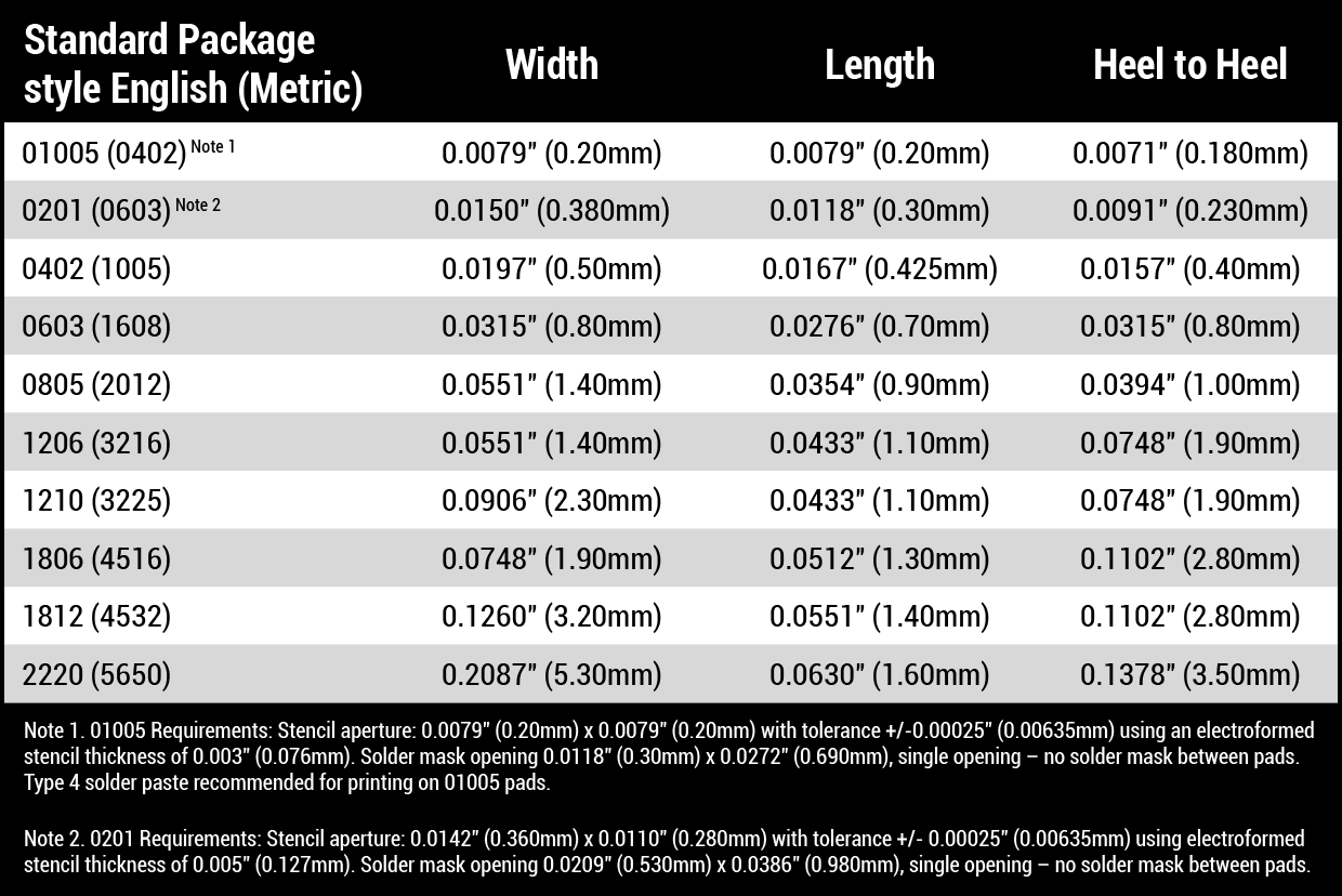
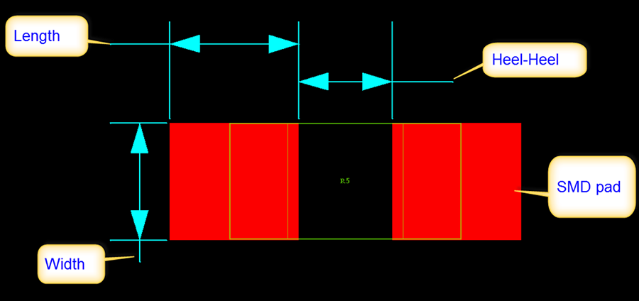
Figure 3. Solder mask clearance recommendations.
Note that every fabricator and assembler has specifications for their specific processes. These specs account for component lead pitch, lead length and body size, and will determine pad width and spacing. These specs will cover the entire range of package styles the manufacturer can build, from through-hole to miniature SMT discretes to high-IO-count area arrays.
A final note. Discrete SMT components of size 0402 (1005 metric) or larger should have a solder mask web between the pads within the pad stack. This enhances isolation and reduces the risk of solder shorts caused by solder wicking (Figure 4).
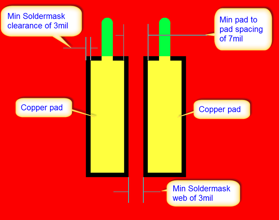
Figure 4. SMT passive land pattern dimensions.
Akber Roy is chief executive of Rush PCB Inc., a printed circuit design, fabrication and assembly company (rushpcb.com); This email address is being protected from spambots. You need JavaScript enabled to view it..


