Solder bridging, PCB copper weight and surface finish: a cause and effect relationship.
Design tends to drive manufacturing, but both continue to push the limits of technology. A good design is one that meets, or exceeds, customer requirements while staying within the capabilities of manufacturing. Divergence from either will affect both.
The majority of defects in a surface mount technology assembly process are introduced at the solder paste printing process. These defects are not always immediately seen and are not solely due to the printer settings, solder paste, stencil or PCB. In some cases, the defects will not be identified until after pick-and-place or after SMT reflow, but, for many, the root cause can be traced to solder paste printing.
One such defect is solder bridging at reflow when printing PCBs with heavy/thick copper and/or a hot-air leveled (HASL) surface finish. The paste print can appear fine, visually, but the solder paste volume is larger than expected. In some cases, enough extra solder paste is printed to force solder bridging in reflow.
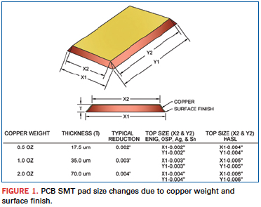
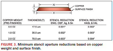
Etching of copper during PCB manufacturing will produce a trapezoidal cross-section (Figure 1) where the top of the SMT pad will be smaller than the bottom. Heavier copper weights are due to a thicker copper layer, and etching thicker copper will produce more of a size difference from top-to-bottom. The bottom (X1 in Figure 1) of the copper is where the measurements are taken during fabrication, and the bottom of the SMT pads will closely match the sizes in the digital PCB files. However, the top of the SMT pad is where paste is printed. Larger reductions at the top of the SMT pad, due to heavy copper etching, can make it more difficult to prevent paste from squeezing out between the PCB and stencil during print.
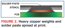
The majority of stencil design rules do not consider copper weight when determining stencil aperture reduction. The stencil aperture width is reduced by a standard amount, regardless of PCB configuration, and is typically tied to component pitch, component type or the SMT land pad size in the Gerber files. However, heavier/thicker copper weights can eliminate the gasket between PCB and stencil. In these cases, a more aggressive width reduction to stencil apertures is required to minimize the opportunity for solder paste squeezing out between the PCB and stencil (Figure 2). If the stencil aperture reductions do not consider the copper weight, the solder volume deposited at print can be quite higher than what is expected. In some cases, there is enough extra solder volume to cause bridging during reflow.
A similar scenario is created when using non-flat surface finishes like HASL and hot-air leveled (HAL). The non-flat surface makes it more difficult to create the gasket between the PCB and stencil and, again, solder paste can squeeze out between the two at print. A reduction to the stencil apertures, based on copper weight, is required, as well as an additional reduction when the surface finish is HASL or HAL. (See Figure 3 for recommended reductions based on copper weight and surface finish.)
Finally, incorporate PCB copper weight and PCB surface finish in stencil design. This cannot only solve potential problems at solder paste print, but also unforeseen problems down the assembly line.
Have you registered for PCB West, the Silicon Valley's largest printed circuit board trade show? Sept. 24-26, at the Santa Clara Convention Center. www.pcbwest.com
And why Thailand holds more promise than Brazil or India.
This is the 15th NTI-100 report, believe it or not. Readers know that over that period, the landscape of the printed circuit board industry has changed. A look at the data compiled in this annual article shows just how dramatic that transformation has been.
As in the past, the author started to collect company revenue data at the end of September 2012. He worked on it on and off for the past nine months, sometimes occasionally, sometimes intensely. In the past two months, the work has been very intensive since most Japanese financial data became available in May and June.
Compiling the NTI-100 becomes more difficult every year as globalization continues and most of the largest fabricators produce printed circuit boards in multiple countries and at multiple locations. Usually, design cost, die cost, shipping cost and insurance are part of sales revenue. (Some fabricators do not include shipping charges.) Most large flex circuit (FPC) manufacturers include in their numbers a substantial amount of FPC assembly, which is difficult to separate from the total output because assembly is very much an integral part of business for those firms. The assembly portion of revenue, if any, is eliminated from the rigid board fabricators. Therefore, the rankings are “unfair” when FPC and rigid board fabricators are compared, but there is no other way. The rankings, then, are “about” rather than definitive. The final judgment is left to the reader.
The table may contain some errors due to oversight or incorrect interpretation of data. The author takes full responsibility for any errors that may exist. Using this opportunity, he would like to express appreciation to those PCB fabricators that provided precious data, and the TPCA and CPCA trade associations for providing valuable information.
Assumptions. Revenues are based on fiscal 2012. Keep in mind, most Japanese companies end their fiscal years on March 31. AT&S also ends its fiscal year on March 31. Some fabricators such as Sanmina and MFlex end their fiscal years at the end of September. There were a number of acquisitions during the course of 2012. To make calculations easier, all acquisitions are assumed to have taken place on Jan. 1. For example, Viasystems acquired DDi on May 31, but its revenue is calculated as if the acquisition took place on Jan. 1.
To reiterate, many FPC fabricators, particularly large ones, engage in assembly. Since assembly is an integral part of their business and it is very difficult to accurately separate assembly-related sales from the total revenue, in these cases no attempt was made to separate the assembly portion. Known assembly revenue has been eliminated from rigid board fabricators.
Average exchange rates. Unfortunately, a common currency must be used for comparison. As usual, the US dollar is used (Table 1). Some discrepancies are unavoidable. For example, Taiwan PCB fabricators convert sales made in China from RMB to NT dollars. Each maker seems to use slightly different exchange rates, and Taiwan and China output are combined as “consolidated” revenue. Then, the author must convert revenues in NT dollars to US dollars. In so doing, some unavoidable discrepancies or errors occur.
To compare growth rates of each maker prior to converting to US dollars, 2011 revenues are recalculated using 2012 exchange rates (local currency comparison). Hence, 2011 data may be different from the last year’s figures. Be forewarned.
Analysis of Top Fabricators
In 2012 the world PCB output was $59.8 billion, down 0.21% from the 2011 output of $59.9 billion, or practically unchanged. The estimated number of PCB fabricators in the world is about 3,000. The number of fabricators that topped $100 million or more in revenue was 106, accounting for only 3.5% of total. For those top 106 fabricators, however, the aggregate output was 81.3% of the total world output in 2011 and 83.4% in 2012. Here, at least, the proverbial 80:20 rule – in which 20% of the manufacturers would be responsible for 80% of the output – does not apply. The big get bigger.
Thirteen fabricators in 2011 had revenues of $1 billion or more. There were also 13 fabricators in 2012, including two new entries and two dropouts. Kingboard Chemical PCB group and CMK fell below the mark. However, CMK became profitable despite the lower revenue thanks to its “select and concentrate” policy. Sumitomo Denko Printed Circuit joined the “NTI-100 $1B Club” thanks to brisk business from Apple. And Viasystems topped the $1 billion mark on the back of the DDi acquisition.
Because of the high value of the yen against the US dollar, Japan had the highest number of entries (28), two ahead of Taiwan (Table 2). However, because the yen is likely to remain at 100:$1 in 2013, Japanese fabricators will slide in the 2013 rankings, and some will likely drop from the list. Japan is the only country whose top fabricators lost revenue in 2012. The number of Hong Kong and China fabricators climbed to 25, almost the same as Taiwan, but the total revenue of these 25 fabricators in 2012 was only one-third that of the 26 Taiwan fabricators. Although Chinese fabricators are growing fast, there is still a long way to go. South Korean fabricators performed the best last year: a whopping growth rate of 25%. Without this, the 2012 world output would have been deeply negative. Samsung Electronics was and is the driver for the Korean PCB industry.
It is said that there are about 100 Taiwanese fabricators, although some have plants only in China. Their total output in 2012 accounted for 33% of the world output. Japan, which once enjoyed the top position with a 32% world share, is now down to a 22% to 23% share, a distant number two to Taiwan. Table 2 hints at this trend.
Table 3 shows revenues sorted by 20th percentiles. Fabricators ranked 1 to 20 and 41 to 60 show the highest growth. Why? Apple and Samsung. Several suppliers in these two categories cater to Apple and Samsung. Their revenues would have been greater if they were not forced to accept continuous price pressure from these users, by the way. Suppliers to Apple and Samsung love the volumes but hate the relentless price pressure. They treat PCBs as “commodities.”
The first NTI-100 article was published in 1998, 15 years ago. The top 100 fabricators then had a total output of $20.2 billion. 2012 saw an output 2.5 times larger. The author would like to continue this work for five more years and then quit. Wish him luck!
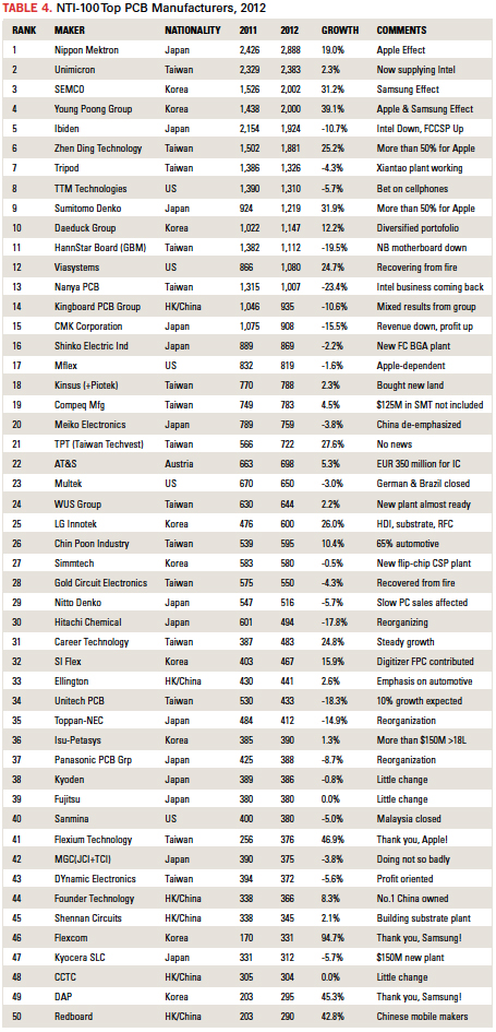
Table 4 is, of course, the NTI-100. Readers may note the absence of Biloda (鑫華寶訊). It turns out that Elitegroup Computer Systems (精英電脳), Biloda’s parent, sold it to a Chinese firm, which in turn shut it down. Elitegroup’s manufacturing arm is “英科技” in Chinese, which contains a PCB manufacturing unit. However, this author could not get data from this business unit.
BYD (比亜連) is a Chinese jack-of-all-trades manufacturer of batteries, automobiles, cellphones and flex circuits, among other things. The author saw an article that pegged its flex business at $250 million. However, since the revenue figure could not be confirmed, BYD was omitted.
HannStar Board (瀚宇博徳) contains GBM (PCB manufacturing operations at four different locations – Shenzhen, Dongguang, Kunshan and the brand new Chongqing factory). HannStar Board Group’s total revenue was approximately $1.8 billion, but about $700 million came from GBM’s rigid board assembly operation, which was subtracted.
TPT-Taiwan Techvest (志超) purchased Yang An (統盟). In TPCA enumeration, TPT and Yang An are listed separately. TPT’s financial data indicate a “consolidated” figure. Since, the author could not reach TPT nor Yang An, they are listed separately.
Despite help from TPCA and CPCA, Taiwan and China fabricators are very difficult to figure out. Within China, a substantial number of mergers and acquisitions seem to take place, which makes it more difficult to collect “consolidated” data.
Young Poong Group, which consists of Young Poong Electronics, Interflex, Korea Circuit and Terranics, showed tremendous growth, thanks to strong orders from Apple and Samsung. A major part of its growth came from its FPC units, Interflex and Young Poong Electronics.
Domestic production by Japanese fabricators continues to decline while the overseas portion continues to increase as most investment is made overseas. Japanese PCB fabricators seem to have ceased investment in China, switching their emphasis to Thailand and Vietnam, and perhaps the Philippines in the future. Several Japanese PCB fabricators operate in Malaysia, but the only one investing is Ibiden.
The trend of the Japanese PCB industry resembles that of North America. Today, the output of the seven largest US-based fabricators is greater than the domestic production of the other 300. To grow in North America, the only choice is to acquire competitors, unless fabricators are willing to invest in capacity, which this author doubts will occur, at least in the near future. In 2000, North America produced $12 billion and employed 97,000 workers. In 2012, the production was $3 billion, and employment was 21,000.
The European situation seems to be more or less the same as North America’s. Nobody in Europe is investing in capacity. Multek Germany is being shut down. eXception Circuit in UK was bought by Fast Print of China. Consider: 5% growth in Europe adds only $120 million to the top line, while 5% growth in China contributes $1.3 billion to the world output. According to its annual report, 74% of AT&S’s revenue was obtained from Asian operations (China, India, South Korea). It is shutting down its Klagenfurt plant; with that move, the last of the former Philips PCB shops will be gone: Eindhoven, Croydon, Evreaux (acquired by Aspocomp and shuttered) and now Klagenfurt. Since AT&S has built a large, new plant in Chongqing, China, more than 85% to 90% of its revenue is likely to come from Asia in the future.
This author is often asked about India and Brazil. Both countries have large populations and their electronics industries are growing. How about PCBs? Domestic fabricators have no ability to invest the large sums seen in China and elsewhere. It is too risky to invest large amounts in PCB manufacture in these countries because of the lack of infrastructure and, to some degree, the political situations. A shortage of quality water and electric power in India are disincentives to large international PCB fabricators. The political situation (taxes, etc.) in Brazil makes large investment impossible. Multek’s money-losing shop in Brazil was closed and its equipment auctioned. Result: One-half of Brazil’s output is gone. Hence, there is no chance any fabricators in India and Brazil will make the NTI-100 list in the foreseeable future.
KCE is building a large plant in Lat Kraban, Thailand, near the new Bangkok International Airport. When the last phase is finished at this new plant, the total production capacity of KCE is expected to be about 5 million sq. ft. a month. Potentially, KCE may achieve $500 million in output in the years to come. What is happening to MFS? Gul Technology has plants only in China. It has done fairly well considering its limited space. Shye Feng Group of Taiwan includes APEX in Thailand (separately stock-listed in Taiwan Stock Exchange), which is also doubling its capacity. Nippon Mektron’s Thai subsidiary, Mektec Thailand, built a new back-end processing plant in Thailand. Canon Components, which quit PCB operations in 2000, built a new plant in Thailand. Fujikura, which was devastated during 2011 “flooding of the century” rebuilt two plants, as well as a new one 28 meters above sea level. Fujikura is aiming to achieve $600 million output in 2015. Considering these investments, the PCB output of Thailand could match that of Europe in a few years. However, all large fabricators in Thailand are Japanese and Taiwanese. Therefore, KCE Electronics is the only domestic entry in the NTI-100.
The author assures readers that the 2013 NTI-100 list will be quite different from the 2012 edition.
Have you registered for PCB West, the Silicon Valley's largest printed circuit board trade show? Sept. 24-26, at the Santa Clara Convention Center. www.pcbwest.com
The Japanese Ministry of Economy, Trading and Industry (METI) released June’s production data for the printed circuit board industry. We now have a six month snapshot for sales in 2013, and can forecast second-half results.
Read more: Japanese Circuit Board Industry Sales, H1 2013
We are often asked about how best to set PCB constraints for double-data-rate (DDR) memory, and how to route to those constraints. This question arose recently when we were asked to create a common style of DDR3 design for training, and we tried mining the web for detailed information on PCB constraints. There had to be something out there, we thought.
Read more: Defining and Routing PCB Constraints for DDR3 Memory Circuits: How-to Movies
In my time working with companies in the automotive, telecom/wireless and defense industries, I often hear of the many issues facing design teams as they tackle projects made up of multiple PCBs connected by flexible PCBs, cables, or with a backplane board.
Read more: Top Tips for Multi-board Design Using a System-level Approach
“Alternatives to Solder in Interconnect, Packaging and Assembly”
Authors: Herbert J. Neuhaus, Ph.D., and Charles E. Bauer, Ph.D.; This email address is being protected from spambots. You need JavaScript enabled to view it.. Abstract: The intense search for attractive lead-free solders reveals the preeminent importance of solder to the industry. In fact, solder consumes so much attention that solder-less alternatives are often overlooked. Material-based alternatives to solder include conductive adhesives and transient-phase compounds. Developments in nanotechnology spawned a virtual renaissance in conductive adhesives and other solder-less joining materials. As a complement to the solder-less materials developments, embedded assemblies use conventional materials in novel ways to improve performance by cutting interconnect parasitics and increase reliability gains by eliminating wire-bonds and solder-bumps. Freescale, Imbera, GE, Verdant and many others develop and employ diverse approaches to embedding active devices. Particle Interconnect represents another solder alternative. While originally developed for automated test, particle interconnect holds considerable promise in a variety of applications, including LED assembly and printed electronics. This presentation surveys the landscape of alternatives to solder in interconnect, packaging, and assembly. It treats practical implementation challenges such as yield management strategies and supply-chain restructuring. Finally, it concludes with a discussion of scenarios in which solder alternatives offer highly compelling business and technical benefits. (SMTA Journal of SMT, vol. 26, no. 1)
Authors: W. Kpobie, N. Bonfoh, C. Dreistadt, M. Fendler, and P. Lipinski; This email address is being protected from spambots. You need JavaScript enabled to view it.. Abstract: Flip-chip technology is increasingly prevalent in electronics assembly 3D system-in-package and is mainly used at fine pitch for manufacture of megapixel large focal-plane detector arrays. To estimate the reliability of these assemblies, numerical simulations based on finite-element methods appear to be the cheapest approach. However, very large assemblies contain more than one million solder bumps, and the optimization process of such structures through numerical simulations turns out to be a very time-consuming task. In many applications, the interconnection layer of such flip-chip assemblies consists of solder bumps embedded in epoxy filler. For such configurations, we propose an alternative approach, which consists of replacing this heterogeneous interconnection layer by a homogeneous equivalent material (HEM). A micromechanical model for the estimation of its equivalent thermoelastic properties has been developed. The obtained constitutive law of the HEM was then implemented in finite-element software (Abaqus). Thermomechanical responses of tested assemblies submitted to loads corresponding to manufacturing conditions have been analyzed. The homogenization–localization process allowed estimation of the mean values of stresses and strains in each phase of the interconnection layer. To access more precisely the stress and strain fields in these phases, two models of structural zoom, taking into account the real solder bump geometry, have been tested. The obtained local stress and strain fields corroborate the experimentally observed damage initiation of the solder bumps. (Journal of Electronic Materials, July 2013)
Reliability
“SnAgCu Lead-Free Electronics Reliability under Combined Temperature and Vibration Environments”
Authors: Pradeep Lall and Geeta Limaye; This email address is being protected from spambots. You need JavaScript enabled to view it.. Abstract: Electronics installed in automotive systems are subjected simultaneously to mechanical vibrations and thermal loads in underhood applications. Typical failure modes include solder joint failure, pad cratering, chip-cracking, copper trace fracture, and underfill fillet failures. The solder interconnects accrue damage much faster when vibrated at elevated temperatures. Presently, the literature on mechanical behavior of lead-free alloys under simultaneous harsh environment of high-temperature vibration is sparse. In this paper, a test vehicle with a variety of lead-free SAC 305 daisy-chain components, including BGA, QFP, SOP, TSOP, has been tested to failure by subjecting it to two elevated temperatures and harmonic vibrations at its first natural frequency. The test matrix includes variation in the amplitude of vibration from 10G to 14G, as well as variation in temperature. Full field strain on the PCB has been extracted using high-speed cameras operating at 100,000 fps in conjunction with digital image correlation. The vibration simulation using global-local finite element models is correlated with the system characteristics such as modal shapes and natural frequencies. The vibration simulation provides a fatigue life prediction that has been validated with the experimentally obtained cycles to failure. In addition, the packages have been cross-sectioned to study the failure modes. A comparison of failure modes for different surface mount packages at elevated test temperatures and vibration is also presented. (SMTA Journal of SMT, vol. 26, no. 1)
This column provides abstracts from recent industry conferences and company white papers. Our goal is to provide an added opportunity for readers to keep abreast of technology and business trends.