A novel process eliminates copper plating, potentially increasing board flexibility and reliability.
A new flexible printed circuit uses circuit layers connected by conductive paste. The technology is based on metal nanoparticle technology developed by Sumitomo.
The method, called paste via method, consists of forming a circuit, drilling holes in the insulating film, and filling the holes with conductive paste. Since the paste via method does not use copper plating, it reportedly reduces the thickness of circuit boards by nearly 30% compared with that of traditional boards, Sumitomo Electric Industries says.
The newly developed FPC is expected to improve the wiring design flexibility of mobile terminals and other electronics devices, and to save space.
A flex circuit is a flexible wiring material consisting of an insulating film on which an electric circuit (conductor layer) is formed using copper foil. The FPC is thin, light and features superior heat resistance, while enabling various parts to be mounted on it. FPCs include single-sided boards (single-layer circuits), double-sided boards (two layers of circuits with insulating film in between), or multilayer boards (three or more layers of circuits) (Figure 1).
[Ed.: To enlarge the figure, right-click on it, then click View Image, then left-click on the figure.]
Conventionally, panel plating (Figure 2) has been widely used to connect the circuits on a double-sided or multilayer board. Panel plating consists of 1) drilling holes in the insulating film, 2) adding two types of conductive copper plating, and 3) forming a circuit. The method is seen as limited in forming precise circuit patterns due to the thickness of the plated copper layers.
In contrast, the paste via method for connecting circuits with conductive paste consists of 1) forming a circuit, 2) drilling holes in the insulating film, and 3) filling the holes with conductive paste. Use of conductive paste and the development of a patent-pending technology that can accurately and evenly fill the paste into the vias enhance circuit connection reliability and boost product quality. Since the paste via method does not use copper plating, it reduces the thickness of circuit boards by nearly 30% compared with that of traditional boards, thereby improving the flexibility of the circuit boards and permitting the formation of more precise circuits. Compared with panel plating, paste via method has simplified flex circuit production and produces higher quality boards.
In April, the firm started full-scale operation of its mass-production line at Minakuchi Works, and has recently started to ship the double-sided FPCs.
Mike Buetow is editor in chief of PCD&F; This email address is being protected from spambots. You need JavaScript enabled to view it..
How a designer/assembler migrated from conventional layout to a more efficient, concurrent DfM process.
Optimum Design Associates designs printed circuit boards following a standardized design flow to ensure customer requirements are met, quality levels are high, and the designs suitable for fabrication, assembly and test.
Optimum is implementing Lean NPI, which we believe is the only way to survive in the competitive field of PCB design and manufacturing. While the process is not yet fully implemented, we describe our journey and near-term plans as a template for what we believe will be the standard procedure for electronics product design.
Optimum’s vision is to offer customers a service following the “Lean New Product Introduction (NPI)” product development model. Lean NPI combines concurrent DfM analysis using vendor-supplied rule sets during the PCB layout process and the adoption of intelligent data transfer as the manufacturing output for hand-off to fabrication and assembly.
The Lean NPI process will provide a number of benefits to Optimum, including reduced time-to-manufacture, increased quality, and easier management of data packaging and handling.
We have already begun the Lean NPI journey by employing concurrent DfM during the PCB layout flow. Running DfM at key stages in the design saves time and effort during NPI. In the final step of Lean NPI adoption, working closely with manufacturing vendors and running DfM based on their rules will show improvements in quality and yield.
Let’s look at Optimum’s PCB design flow and transfer to manufacturing before a more detailed look at Lean NPI and its implementation.
PCB design process. Although Optimum has several PCB design tools available, depending on customer compatibility and fabricator requirements, Mentor Graphics tools have been the mainstay since the business was founded in 1991. Currently, we employ Expedition Enterprise and PADS.
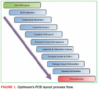
The PCB layout process flow used at Optimum is shown in Figure 1. When PCB layout begins, the first step is to validate the bill of materials (BoM) using Mentor Graphics Valor NPI and Valor Parts Library to check that all part numbers, reference designators and quantities are correct and that package models are available for later use in the design flow. Missing package models can be generated at this early stage. Once component placement is completed, the design is subject to DfM verification using the same tools.
On completion of layout, provisional outputs are generated and delivered to the customer for design approval. In parallel, a comprehensive fabrication and assembly DfM analysis is performed. The results are used to confirm that there will be no quality or process issues during fabrication and assembly of the product and to ensure maximum possible yield.
Some companies do not use DfM analysis until the design reaches the fabricator, primarily to ensure acceptable yields of bare boards. If significant problems are found, the project must go back to design for a re-layout and then back to the fabricator. This can take days or weeks and incur a hefty cost.
Optimum has embraced the concept of concurrent DfM within the PCB layout process flow. By moving the DfM as early in the product design as possible – running partial checks on available data – problems are relatively easy to correct, and cost very little in either time or money compared to having a complete re-spin. At key stages of the design, the layout is examined at multiple points to assess the viability of both fabrication and assembly, which ensures the design meets the capabilities and process constraints of the manufacturer.
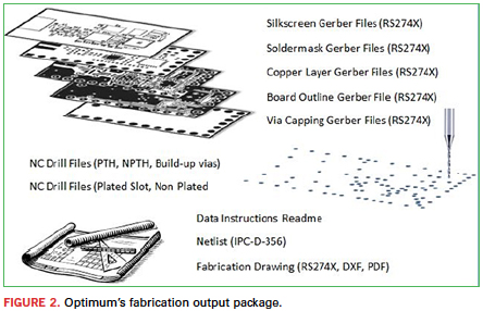
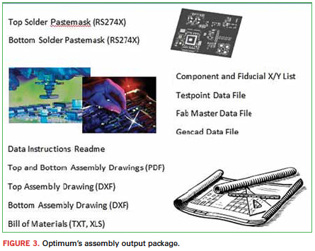
The last step in the PCB design phase is compiling the electronic files to deliver to the fabricator. Optimum produces an ODB++ output file as well as Gerber-based file sets. To ensure consistency between the DfM-verified ODB++ data and the traditional Gerber and Excellon drill outputs, Optimum conducts a graphical comparison. Once verified that both output formats are graphically identical, the final deliverable data are packaged and released to the customer and the fabricator. In addition to producing data packages for fabrication (Figure 2), Optimum produces assembly (Figure 3) data packages.
The aforementioned might be called the “standard” NPI process; that is, what most leading designers and fabricators are implementing today. As we described, Lean NPI is the next segment in the journey to become a complete Lean NPI-driven design and manufacturing entity. There are various levels of DfM that can be executed during the NPI process:
Level 0 DfM is performed on the factory floor where the product build is attempted and DfM problems are discovered. This method of verification is time-consuming and expensive.
Level 1 DfM is performed by the manufacturer using software tools and is a reasonable method to ensure the design complies with manufacturing rules and process constraints. The downside to this level is that the design organization is completely reliant on DfM feedback from the manufacturer. This feedback is used to make necessary design changes but may not include details about the design that could affect product yield or reliability.
Level 2 DfM is the ideal scenario, where DfM is executed during the design process using manufacturer-derived rules and process constraints. Not only can critical DfM errors be addressed during design, but improvements can be made to increase yield and reliability before committing to production runs. The most efficient method of implementing DfM is to adopt concurrent DfM engineering. The PCB layout is designed in stages: placement, critical routing, final routing/planes. At each of these key stages: DfM analysis is executed. It can be very difficult and time-consuming to correct DfM problems after the layout is complete.1
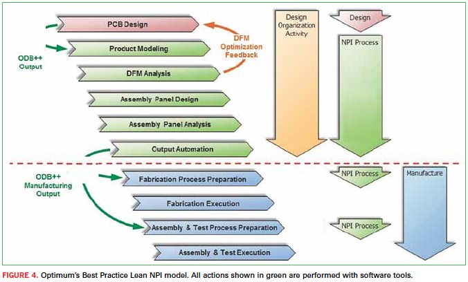
Best practice Lean NPI process model. Lean NPI is defined by three enhancement elements within the “Best Practice Standard NPI Process Model.” First, ODB++ data are used as the preferred format for manufacturing hand-off because it contains product model intelligence, thus enabling high levels of automation. The second element is to execute concurrent DfM at key stages during PCB design development. The final element for Lean NPI is to execute DfM at Level 2. Figure 4 shows Optimum’s model, which is the template to which we are working.
[Ed.: To enlarge the figure, right-click on it, then click View Image, then left-click on the figure.]
The layout is designed in stages and concurrent Level 2 DfM analysis is executed. When the layout is complete and any DfM problems resolved, the assembly panel is designed and validated. The final manufacturing output is generated and released for manufacturing process preparation.
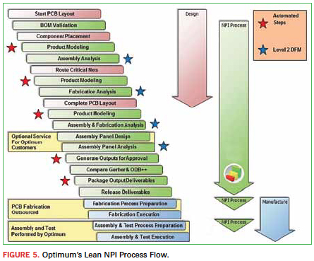
Lean NPI process flow. During the collaboration with Mentor, some areas of Optimum’s business process have been identified where improvements can be made to achieve Lean NPI. By merging our PCB layout process flow with the Lean NPI process model, we derived the Lean NPI Process Flow (Figure 5). Although it may appear complex at first, many of the steps in the flow are fully automated.
At the beginning of the design, the BoM is validated. This ensures all packages are available. If new packages are required, these can be generated while the component placement is performed. The completed placement is then subject to initial assembly analysis.
If DfM problems exist, they can be fixed before continuing with any complex routing. Prior to each analysis stage, product modeling adds attributes to the manufacturing data, which enables comprehensive DfM checks to be executed, and also defines exactly what is to be manufactured such as layer stackup, copper weights, solder mask color and component assembly instructions. This removes the need for many drawings and documents traditionally used to communicate deliverables to the manufacturer. All product modeling activities are automated and repeatable.
Any critical routing can then be added to the design. On completion of the critical routing, an initial fabrication analysis is run. This highlights any DfM problems associated with the critical nets that need correcting before continuing with general routing. Clearly, critical routing should not be disturbed at a later stage due to DfM problems, as it may be very difficult to make changes while retaining signal integrity.
Next, the remainder of the routing, copper areas, power and ground planes and silkscreen legend (if applicable) can be completed. A final DfM analysis is run for fabrication, assembly and test that captures any DfM problems with the completed layout.
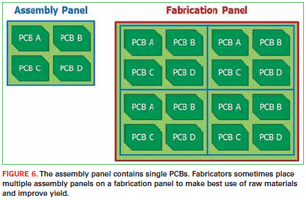
Once all DfM problems are investigated and corrected on the single PCB design, the assembly panel design and panel DfM analysis can be performed. This is an optional step offered by Optimum. Figure 6 illustrates the difference between the assembly panel and fabrication panel. The assembly panel is the fabricator’s deliverable and is used by the PCB assemblers. The assembly panel usually contains an array of single circuit boards. The fabrication panel contains an array of assembly panels and is only used to suit the fabrication processes and make best use of their raw materials.
Finally, the complete data package goes to the customer for final approval. During the approval process, if the customer requires Gerber data, we compare the Gerber output against the master ODB++ output to ensure that the data are graphically identical. Thus, the traditional Gerber data can still be used as a valid if less-efficient alternative in manufacturing process preparation. On receipt of customer design approval, the final manufacturing data are packaged and delivered to the manufacturer.
Remaining steps. During study of the PCB layout process flow, areas were identified where changes could be made to fully implement the Lean NPI process model. Key areas where Optimum’s business process could be modified are:
Optimum’s PCB design and NPI process would be enhanced by adding a DfM analysis stage when the critical routing is complete. This would ensure no DfM problems exist with the critical nets. If DfM problems do exist, they could be corrected and signal integrity retained. If DfM problems are discovered with the critical nets at a later stage it may be difficult and time-consuming to fix the problems without disturbing other routing or even component placement while retaining signal integrity.
The customer-approval stage could be moved to after the final fabrication and assembly DfM analysis step. This will ensure that the output data used for customer review and approval not only meet the electronic design specifications but are also fully manufacturing-compliant. Otherwise, changes may need to be made during the final DfM validation stage that the customer may not be aware of. This change to the process flow will also enable the customer to check and approve the manufacturing data – exactly what is to be manufactured.
Ensure exclusive use of ODB++ output data format throughout the flow from design to manufacturing process preparation. This would enable a more efficient data hand-off to both Optimum’s external fabrication partners and internal assembly and test lines.
As with any significant changes in design methods or business processes, there need to be metrics in place to measure performance improvements and show the effect of those changes on the performance of the business. We are currently developing and will be compiling performance and quality metrics that will be analyzed and discussed in a future article.
References
1. Matt Kelly and Mark Hoffmeyer, “Lead-Free Assembly Design for Manufacturability Considerations,” PCD&F/CIRCUITS ASSEMBLY, February 2013.
Randy Holt is a senior PCB designer at Optimum Design Associates and a former “Top Gun” winner at PCB West; This email address is being protected from spambots. You need JavaScript enabled to view it..
The world’s largest electronics show for Electronics Packaging, Circuits and Assembling (the JPCA Show) was held at Tokyo Big Sight from June 5 through June 7. The following shows were held concurrently in the convention center: Large Electronics Show 2013, JIEP 2013 (Microelectronics Show), Jisso Protech 2013 and Monotsukuri Fiesta 2013. The electronics industry in Japan is suffering its worst slump in history. I was hoping to see some new and innovative products at the show to snap us out of this funk.
It’s no secret that placing passive devices in the proper location, whether nearer to the source/driver or the receiver/load pins, is the difference between poor signal integrity and optimal signal integrity. Often this can be impacted by a breakdown in communications between circuit designers and PCB designers.
Read more: Achieving Proper Placement of Passive Devices Used for Enet Signal Termination
Where AOI and conventional x-ray peak, other methods can hone in on nettlesome defects.
X-ray and AOI, along with related equipment, have long been the stalwarts of post-placement printed circuit board inspection. Over the years, as packaging, device and board technologies have advanced, these inspection technologies have advanced as well to present the best inspection results possible based on the technology of the day. These inspection machines are nondestructive, meaning PCBs and their components remain intact while being inspected for failure analysis.
Certainly, even the simplest of inspection tools, the digital camera, with specialized lighting systems, continues to prove valuable for a number of tasks. Those include checking for cosmetic errors, verifying a component’s numbering system, viewing surface finish corrosion and half moons on the via sites, determining if the gold surface is peeling away from a board’s surface, whether the drill is properly controlled, viewing the dimples of delaminations, and a host of other potential problems. Some may be cosmetic in nature, but others could cause severe damage to the board.
Automatic optical inspection, programmed with the so-called golden (perfectly assembled) boards, compares that specimen with others that follow to capture design flaws or defects. It also catches defects such as wrong polarity, missing components, wrong components and incorrect orientation.
AOI continues to get smarter at catching board problems on the assembly floor. Newer generation machines have as many as six cameras, and offer side angle viewing of specific markings to observe components. State-of-the-art AOI comes with brighter LED lighting systems and, aided by software advances, captures a considerably better image and also detects greater numbers of accurate failures and fewer false failures.
In many cases, both conventional and automated x-ray inspection (AXI) are used on the assembly floor. AXI is used for leading-edge technologies such as ball grid arrays (BGAs), chip-scale packaging, flip chips, QFNs, DFNs, and others. It shines radiation through a component package such as a BGA to reveal whether balls are soldered properly to the PCB. Standard x-ray inspection is used for simple applications, whereas high-end x-ray is used to detect such tough-to-find defects as head-in-pillow, disjointed balls on a BGA package, wire bonding damage, and other similar problems.
These post-assembly inspection machines are precisely engineered for the tasks they are intended to perform. However, there exists one more hurdle to overcome given today’s design and technology demands: The current basic inspection issue or obstacle lies squarely on image processing. Image capturing is the easy part of the two; however, the biggest challenge is effectively capturing an image in low light. That’s not possible due to a high signal-to-noise ratio (SNR) in the design of current inspection systems. On the other hand, a lower SNR suppresses noise and increases and enhances an image. The challenge is for inspection system designers to suppress that excessive noise so that SNR is within acceptable limits.
However, today, with the rapidly escalating use of smaller, more complex packaging like µBGAs, µCSPs, and package on package (PoP), conventional inspection tools and their supporting technologies are finding it difficult to stay ahead of the demands smaller packaging and shrinking board sizes pose.
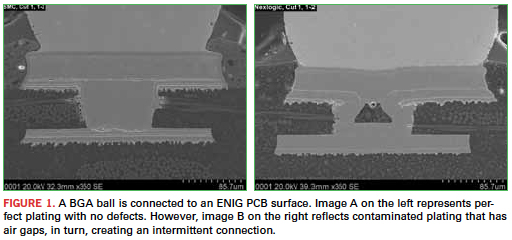
Consequently, the industry has to go deeper into these smaller PCBs and their small components to minutely strip away obstacles to view the tiniest of crevices to conduct failure analysis via forensics. For example, as shown in Figure 1, a BGA ball is connected to an ENIG PCB surface. Image A on the left represents perfect plating with no defects. Image B on the right reflects contaminated plating that has air gaps, in turn, creating an intermittent connection.
[Ed.: To enlarge the figure, right-click on it, then click View Image, then left-click on the figure.]
The absence of forensic analysis tools and techniques puts ample time (rework and product delays) and money (in labor and materials) at risk.
In response, conventional nondestructive inspection is partnering with forensics analysis to do detective work and sleuth around the insides of a package on package (PoP), for example. This newest of inspection techniques is increasingly making its way into the assembly floor with its bag of tools to investigate and detect the smallest of culprits causing board defects. The tools include scanning electron microscopy (SEM) and time domain reflectometry (TDR). While this technology isn’t exactly new, some service bureaus use it to specialize in this type of failure analysis. Forensics isn’t in the mainstream of PCB assembly today, but it’s making inroads.
Board Sacrifice
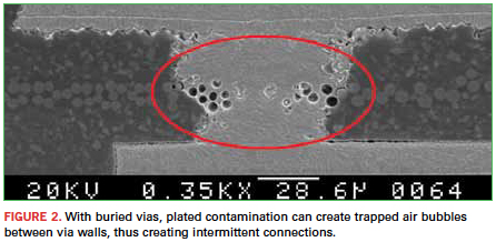
With forensic analysis, more commonly known as destructive inspection, one board from a project order that is demonstrating poor performance is sacrificed for what is essentially an electronics autopsy. That board and the devices populating it are dissected, and extremely high electron microscope magnification views physical cross-sections in pursuit of the problem. For instance, in the case of buried vias, plated contamination can create air bubbles to be trapped between walls of the via, thus creating intermittent connections (Figure 2) that otherwise could not be revealed by conventional inspection.
Forensics analysis comes in at a time when conventional inspection cannot locate the problematic areas. Say x-ray, AOI and specialized high megapixel digital cameras are in use, but yields are below acceptable levels. You’re absolutely sure of your processes, the different flow charts, and of manufacturing. However, you’re not able to pinpoint a certain defect. That’s when forensics comes into play.
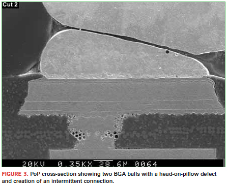
Again, take the PoP as the example. It’s not performing or is failing. The pass rate and yields are extremely low. Here, the cross-section of this PoP plays a central role in failure analysis. It provides physical evidence and root cause of the failure mode, shows the failure site location, and then isolates it from suspected versus non-suspected devices. Figure 3 shows the cross-section of a PoP. Two BGA balls are shown with a head-in-pillow defect, another cause for an intermittent connection.
Forensic analysis uncovers an innumerable number of defects or failures that conventional inspection cannot. At the board level, it investigates thickness of copper plating on the through-holes and vias; if it’s an immersion gold finish, the gold plating thickness can be observed to determine whether an adequate amount of gold has been deposited, per fabrication specs. On an electroless-nickel immersion gold (ENIG) finish, forensic analysis ensures the nickel, which is the base plating before the gold is deposited, is performing according to the spec sheet. Also, it pinpoints infinitesimally minute fractures within solder joints.
Minute solder pinholes are not visible at the 300X to 400X magnification level. But with SEM, those pinholes are magnified upwards to the 2,000 times level. Plus, in some instances, black pads, the acute corrosion of a board’s nickel-plating layer, can be viewed very clearly. Moreover, one of the more elusive issues, particularly with BGAs and µBGAs, is the problem with intermittent connections, meaning a faulty connection between and among a BGA’s balls exists. Forensic analysis can locate these inter-metallic failures, which are the most troublesome when it comes to BGAs in systems out in the field. It can determine the distance between gold plating and the solder ball, in case BGA balls are detached after the assembly process, and also comes to a conclusive analysis when checking organic solderability preservative (OSP) versus gold versus immersion silver board surface finishes.
Solder thermal fatigue and current leakage failures are other specialties forensics excel in. Due to solder thermal fatigue, open circuit failure occurs in the field when a product is subjected to excessive heat, rugged conditions or extreme temperature variations, especially on BGAs or PoP devices. Those defects are especially prevalent in PoP packages because multiple BGA devices are stacked on top of each other, and that process needs to be 100% accurate or else it will create field failures. Those fatigue cracks become more pronounced over time. A solder joint experiencing those cracks eventually detachs from the board’s surface due to the excessive heat. This is especially true if the BGA is not properly assembled.
In some instances, solder bridging of flip-chip devices has leakage failures. After thermal cycling, the device leaks current due to solder or flux; insufficient current arrives at a BGA’s proper ball, and an unacceptable signal is then provided at certain levels. This especially occurs when underfill is used between a solder ball and board surface.
The data developed via forensic methods can then be fed upstream to the designer to respin the board, as necessary.
If quality assurance reveals persistent PCB problems that otherwise cannot be resolved by tweaking the AOI, forensics are the next step to revealing the source of the defect.
Zulki Khan is president and founder of NexLogic Technologies (nexlogic.com); This email address is being protected from spambots. You need JavaScript enabled to view it..