The 2013 Class developed many of the tools still used by PCB designers today.
The father of the gridless router. The largest seller of CAD seats. A leading inventor of team-based design. The foremost signal integrity guru. These are the four latest inductees to the Dieter W. Bergman PCB Design Hall of Fame.
They include two deans of CAD software development: Rich Nedbal, the founder of P-CAD, and the late Alan Finch, of Racal-Redac. The 2013 Class also includes Charles Pfeil, who invented a method for several users to simultaneously edit a single design without, in short, messing everything up. And finally there is Dr. Howard Johnson, the brilliant and relentless signal integrity guru, whose groundbreaking work on mixed signals overshadowed his invention of voicemail.
They join six other legends of the PCB design world in the Dieter W. Bergman PCB Hall of Fame, named for the longtime IPC technical director who has spent more than 40 years lifting the recognition and professionalism of the discipline.
Alan C. Finch is known as the father of the shape-based autorouter. In 1985, Finch, with coauthors K.J. Mackenzie, G.J. Balsdon, and G. Symonds of Racal-Redac, proposed a gridless method for designing fine-line printed circuit boards. The inventors said in their groundbreaking paper, which was presented at the 22nd IEEE Design Automation Conference, that then-current designs had “stretched most previous automatic routing algorithms to the limit.” Building on a concept from 1980 by Ulrich Lauther, the former Racal-Redac developer conceived a router with no defined cell size. The resulting tools forever changed the way printed circuit design is performed. Finch died in late December.
Dr. Howard Johnson is considered the leading authority on signal integrity, having spent much of his career demonstrating the effects of analog signals in high-speed digital systems. He is author of three books, including two on high-speed design, and has taught more than 12,000 students over his 30-plus-year career. As the Institute of Electrical and Electronics Engineers’ chief technical editor, Johnson wrote standards that govern Ethernet, IEEE 802.3 Fast Ethernet and IEEE 802.3 Gigabit Ethernet. In 1979, Johnson invented PhoneMail, the first integrated voice messaging system. During his career, Johnson was manager of technology and advanced development at ROLM, director of engineering at US TeleCenters, and manager of technology and advanced development at Ultra Network Technologies. He has bachelor’s, master’s and doctoral degrees from Rice University.
Richard (Rich) Nedbal is credited with revolutionizing computer-aided manufacturing software for printed circuit fabrication. An electrical engineer who graduated from the University of Illinois at Chicago in 1966, Nedbal worked at Carnegie Mellon Institute from 1970 to 1976, designing system logic and integrated circuits for electronic fuel injection systems prototypes. When the research program ended, Nedbal moved to California and rose through the ranks at American Microsystems, a semiconductor design and manufacturing company. In 1982, he founded Personal CAD Systems, with the goal to develop lower cost electronic CAD tools. By 1988, P-CAD, as the company came to be known, owned the largest installed base of users in the EDA industry, with over 10,000.Two years later, P-CAD had over 100,000 users, at which point Nedbal sold the firm to Accel Technologies.
Having shaken up the CAD industry, Nedbal then set his sights on CAM tools. He founded Advanced CAM Technologies in 1994. At ACT, Nedbal changed the idea of what a CAM tool could be, as its signature tool, called CAM350, was the first CAM tool to adopt many traits of a CAD tool. After Pads Software’s acquisition of ACT, in 1998, Nedbal stayed on for a year, then left the industry to purse a second career building injection systems for car engines.
Charles Pfeil has been a designer, owner of a service bureau, and an engineering manager for a variety of software vendors, including Racal, ASI, Cadence, PADS, VeriBest and Mentor Graphics. He was one of the first to latch on to the concept of team design, and one of his eight patents is for his 2002 invention of parallel electronic design (also known as shared simultaneous editing), a method that allowed multiple users to edit shared areas of a master design while preserving the design integrity. Other patents described distributed autorouting and breakouts. During his 40-plus-year career, Pfeil invented multiple CAD tools (including XtremePCB and XtremeAR, and TeamPCB for Mentor Graphics, where he also was product architect for Expedition PCB). He authored BGA Breakouts and Routing, a well-received book on designing with ball grid arrays.
Mike Buetow is editor in chief of PCD&F; This email address is being protected from spambots. You need JavaScript enabled to view it..
Polyimide pushes the electrical envelope without swelling the form factor.
Mobile devices are a fast-paced, growing market. Flexible printed circuits are a key element in making these devices smaller and thinner, while increasing functionality. Let’s recap how has flex use evolved in the mobile device market.
Flex circuits were originally used as interconnect for features located on different levels within an assembly. By and large, these flexes were relatively simple – not much more than a thin jumper cable. As mobile device designers conjured the “flip phone” form factor, flex circuits fulfilled the need for dynamic bending applications in the hinge of those devices. Flex gained more complex features, with multiple bends and air gaps, some with components placed on them. As assembly increased, flex helped enable “slider phones” with dynamic, rolling features with expanded functions such as full keyboards and larger displays.
As mobile phones competed to be the “smartest” on the block, designers were pressed to cram in a wider range of rich media, connected functionality. Flex allowed designers to fill smartphone chasses with a variety of components and modules with multiple small-radius bends, leading to reinforced zones with metal or plastic for side keys, cameras, displays and more.
Here’s where we are today: thin, flat and highly populated flexible circuit assemblies with a range of components on one or both sides of the board. One of the most important applications is the ability of the boards to bend, flex and be shaped into 3D forms. While these mechanical features enable the addition of new features, it’s the electrical properties of the flexible substrates that play a critical role in enabling the high-definition user experiences we enjoy in mobile devices today.
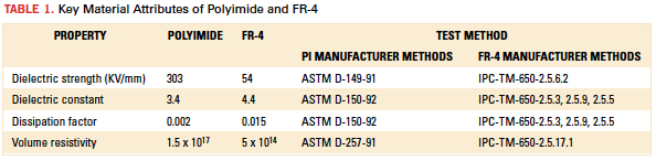
When I look at the electrical properties of polyimides and other thin flexible substrates used in FPC fabrication, I find the electrical properties of FPC dielectrics are often superior to the equivalent FR-4 material sets (Table 1).
[Ed.: To enlarge the figure, right-click on it, then click View Image, then left-click on the figure.]
How do the electrical properties in Table 1 enable the FPC to do what an FPC does: be very thin and bendable while maintaining signal performance? As a dielectric material, polyimide has a few advantages over FR-4, higher dielectric strength and volume resistivity. The dielectric strength is a measure of the electrical performance of a material as an insulator. It is defined as the voltage required to produce a dielectric breakdown through the material. Volume resistivity is the measure of a material's ability to prevent an electrical current through its structure. The higher the surface/volume resistivity, the lower the leakage current and the less conductive the material is. These two properties combined are what enable flex manufacturers to use very thin layers of material between conductors to provide adequate electrical isolation. This advantage works not only in the horizontal plane with conductive traces, but also enables a closer space between adjacent via barrels.
The result: Polyimide’s electrical properties enable FPCs to be 70% thinner than an equivalent PCB.
When looking at the dielectric constant and the dissipation factor, polyimide generally compares quite favorably to FR-4. While I’ve excluded the impedance calculation for the sake of sanity, the takeaway here is that lower dielectric constants (Dk) enable FPCs to maintain larger trace dimensions and thin dielectrics and still maintain the desired impedance control, whereas designers must compensate for materials with a higher DK with finer (and more difficult to produce) traces, as well as thicker dielectrics. As for dissipation factor (Df), the measure of the loss-rate of energy along an insulated conductor, materials with a lower Df enable FPC to achieve impedance requirements and signal integrity, while preserving FPC’s thinness advantage over an FR-4 PCB.
It’s fair to ask, How much difference could there really be? Take a PCB. Reduce the thickness by one-third, then bend it around and under or over that troublesome battery that always seems to be making the designs thicker than your manager wants them.
As we look to the future of new devices with new functions, we believe FPC’s strengths to bend and flex will continue to be a clear value add, but it’s the electrical properties of today’s polyimides, making it possible to achieve controlled impedance and high-frequency performance in a thin and lightweight interconnect that will be of increasing value to electronics product designers.
Simply put, today’s devices have no space to spare, so even if your interconnect application does not need to bend, do not eliminate the FPC as an option. Think of FPC for the thinness and lightness. Use FPC for its high-performance electrical properties. Remember, FPCs are not just for bending anymore.
Dale Wesselmann is a product marketing manager at MFLEX (mflex.com); This email address is being protected from spambots. You need JavaScript enabled to view it.. His column runs bimonthly.
From components to wrist straps, a look at more than 60 documents that make up ESD control programs.
Industry standards play a major role in providing meaningful metrics and common procedures that permit manufacturers, customers and suppliers to communicate from facility to facility around the world. Standards are increasingly important in our global economy. In manufacturing, uniform quality requirements and testing procedures are necessary to make sure all involved are speaking the same language. In ESD device protection, standard methods have been developed for component ESD stress models to measure a component’s sensitivity to electrostatic discharge from various sources. In ESD control programs, standard test methods for product qualification and periodic evaluation of wrist straps, garments, ionizers, worksurfaces, grounding, flooring, shoes, static dissipative planar materials, shielding bags, packaging, electrical soldering/desoldering hand tools, and flooring/footwear systems have been developed to ensure uniformity around the world.
The EOS/ESD Association, Inc. (ESDA) is dedicated to advancing the theory and practice of electrostatic discharge (ESD) protection and avoidance. The ESDA is an American National Standards Institute (ANSI) accredited standards developer. The association’s consensus body is called the Standards Committee (STDCOM), which has responsibility for the overall development of documents. Industry volunteers participate in working groups to develop new and update current ESDA documents.
STDCOM is charged with keeping pace with the industry demands for increased performance. The existing standards, standard test methods, standard practices and technical reports assist in the design and monitoring of the electrostatic protected area (EPA), and also assist in the stress testing of ESD sensitive electronic components. Many existing documents relate to controlling electrostatic charge on personnel and stationary work areas. However, with increasing emphasis on automated handling, the need to evaluate and monitor what is occurring inside of process equipment is growing daily. Since automation has become more dominant, the charged device model (CDM) has become the primary cause of ESD failures and thus the more urgent concern. Together, the human body model (HBM) and charged device model cover the vast majority of ESD events that might occur in a typical factory.
The ESDA document categories are:
Standard (S): A precise statement of a set of requirements to be satisfied by a material, product, system or process that also specifies the procedures for determining whether each of the requirements is satisfied.
Standard Test Method (STM): A definitive procedure for the identification, measurement and evaluation of one or more qualities, characteristics or properties of a material, product, system or process that yield a reproducible test result.
Standard Practice (SP): A procedure for performing one or more operations or functions that may or may not yield a test result. Note: If a test result is obtained, it may not be reproducible.
Technical Report (TR): A collection of technical data or test results published as an informational reference on a specific material, product, system or process.
The ESDA Technology Roadmap is compiled by industry experts in IC protection design and test to provide a look into future ESD design and manufacturing challenges. The roadmap previously pointed out that numerous mainstream electronic parts and components would reach assembly factories with a lower level of ESD protection than could have been expected just a few years earlier. This prediction has proved rather accurate. As with any roadmap, the view of the future is constantly changing and requires updating on the basis of technology trend updates, market forces, supply-chain evolution and field return data. An updated roadmap was published in March, and industry experts extended the horizon beyond the 2013 predictions. It contains, for the first time, a roadmap for the evolution of ESD stress testing. This includes forward-looking views of possible changes in the standard device level tests (HBM and CDM), as well as the expected progress in other important areas, such as transmission line pulsing (TLP), transient latch-up (TLU), cable discharge events (CDE), and charged board events (CBE). A view of work on electrical overstress (EOS) has also been included. EOS is an area that has long been overlooked by the industry, not because it was not important but because it could be a difficult threat to define and mitigate. Recently, a working group has been focusing on this area and will soon be publishing a technical report (TR) that helps establish some fundamental definitions and distinctions between various EOS threats. The TR will be followed by a “best practices” document outlining ways to mitigate EOS threats. Another development has been a request by the aerospace industry for an ESD control document that defines more definitively what ESD controls need to be in place in aerospace manufacturing factories. This document will be predicated on ANSI/ESD S20.20 but will introduce further limits and controls.
The ESDA Standards Committee is continuing several joint document development activities with the JEDEC Solid State Technology Association. Under the memorandum of understanding, the ESDA and JEDEC formed a joint task force for the standardization work. This collaboration has paved the way for development of harmonized test methods for ESD, which will ultimately reduce uncertainty about test standards among manufacturers and suppliers in the solid state industry. At the time of this publication, ANSI/ESDA/JEDEC JS-001-2012, a third revision of the joint HBM document, has been released for distribution. This document replaces ANSI/ESDA/JEDEC JS-001-2011, the current industry test methods and specifications for human body model device testing. A second joint committee is currently working on a joint charged device model (CDM) document with a goal of publishing in 2014. These efforts will assist manufacturers of devices by providing one test method and specification instead of multiple, almost – but not quite – identical, versions of device testing methods.
The ESDA is also working on a process assessment document. The purpose of this document is to describe a set of methodologies, techniques and tools that can be used to characterize a process where ESD-sensitive items are handled. The goal is to characterize the ability of a process to safely handle ESD-sensitive devices that have been characterized by the relevant device testing models. The document will apply to activities that manufacture, process, assemble, install, package, label, service, test, inspect, transport, or otherwise handle electrical or electronic parts, assemblies, and equipment susceptible to damage by electrostatic discharges. At the present time, this document will not apply to electrically initiated explosive devices, flammable liquids or powders.
The ESDA standard covering the requirements for creating and managing an ESD control program is ANSI/ESD S20.20, “ESD Association Standard for the Development of an Electrostatic Discharge Control Program for – Protection of Electrical and Electronic Parts, Assemblies and Equipment (Excluding Electrically Initiated Explosive Devices).” ANSI/ESD S20.20 is a commercial update of and replacement for MIL-STD-1686 and has been adopted by the US Department of Defense. In addition, the 2007-2008 update of IEC 61340-5-1 edition 1.0 “Electrostatics - Part 5-1: Protection of Electronic Devices from Electrostatic Phenomena General Requirements” is technically equivalent to ANSI/ESD S20.20. A five-year review of ANSI/ESD S20.20 has begun, and technical changes are being made to the document based on industry changes and user requests. Unique constraints with the revision must be taken into account, including facility certification and continued harmonization with other standards: IEC 61340-5-1 and newly revised JEDEC 625B. A target date of September 2013 has been given for the release of a draft document.
In order to meet the global need in the electronics industry for technically sound ESD control programs, the ESDA has established an independent third-party certification program. The program is administered by the EOS/ESD Association through country-accredited ISO 9000 certification bodies that have met the requirements of this program. The facility certification program evaluates a facility’s ESD program to ensure that the basic requirements from industry standards ANSI/ESD S20.20 or IEC 61340-5-1 are being followed. More than 519 facilities have been certified worldwide since inception of the program. The factory certification bodies report strong interest in certification to ANSI/ESD S20.20, and consultants in this area report that inquiries for assistance remain at a very high level. Individual education also seems of interest once again, as 46 professionals have obtained Certified ESD Program Manager status, and many more are attempting to qualify as Certified ESD Control Program Managers. A large percentage of the certification program requirements are based on standards and the other related documents produced by the ESD Association Standards Committee.
Current ESD Association Standards Committee Documents
Charged Device Model (CDM). ANSI/ESD S5.3.1-2009 Electrostatic Discharge Sensitivity Testing - Charged Device Model (CDM) - Component Level: Establishes the procedure for testing, evaluating, and classifying the ESD sensitivity of components to the defined CDM.
Cleanrooms. ESD TR55.0-01-04 Electrostatic Guidelines and Considerations for Cleanrooms and Clean Manufacturing: Identifies considerations and provides guidelines for the selection and implementation of materials and processes for electrostatic control in cleanroom and clean manufacturing environments. (Formerly TR11-04)
Compliance verification. ESD TR53-01-06 Compliance Verification of ESD Protective Equipment and Materials: Describes the test methods and instrumentation that can be used to periodically verify the performance of ESD protective equipment and materials.
Electronic design automation (EDA). ESD TR18.0.01-11 – ESD Electronic Design Automation Checks: Provides guidance for EDA industry and ESD design community for establishing a comprehensive ESD electronic design automation verification flow satisfying the ESD design challenges of modern ICs.
ESD control program. ANSI/ESD S20.20-2007 Protection of Electrical and Electronic Parts, Assemblies and Equipment (Excluding Electrically Initiated Explosive Devices): Provides administrative and technical requirements for establishing, implementing, and maintaining an ESD Control Program to protect electrical or electronic parts, assemblies, and equipment susceptible to ESD damage from Human Body Model (HBM) discharges greater than or equal to 100V.
ESD TR 20.20-2008—ESD Handbook (Companion to ANSI/ESD S20.20): Produced specifically to support ANSI/ESD S20.20 ESD Control Program standard, this 132-page document is a major rewrite of the previous handbook. It focuses on providing guidance that can be used for developing, implementing, and monitoring an ESD control program in accordance with S20.20.
Flooring. ANSI/ESD STM7.1-2012 Resistive Characterization of Materials – Floor Materials: Covers measurement of the electrical resistance of various floor materials, such as floor coverings, mats, and floor finishes. It provides test methods for qualifying floor materials before installation or application, and for evaluating and monitoring materials after installation or application.
ESD TR7.0-01-11 Static Protective Floor Materials: This technical report reviews the use of floor materials to dissipate electrostatic charge. It provides an overview on floor coverings, floor finishes, topical antistats, floor mats, paints and coatings. It also covers a variety of other issues related to floor material selection, installation and maintenance.
Flooring and footwear systems. ANSI/ESD STM97.1-2006 Floor Materials and Footwear – Resistance Measurement in Combination with a Person: Provides test methods for measuring the electrical system resistance of floor materials in combination with person wearing static control footwear.
ANSI/ESD STM97.2-2006 Floor Materials and Footwear – Voltage Measurement in Combination with a Person: Provides for measuring the electrostatic voltage on a person in combination with floor materials and footwear, as a system.
Footwear. ANSI/ESD STM9.1-2006 Footwear – Resistive Characterization: Defines a test method for measuring the electrical resistance of shoes used for ESD control in the electronics environment (not to include heel straps and toe grounders).
ESD SP9.2-2003 Footwear – Foot Grounders Resistive Characterization: Provides test methods for evaluating foot grounders and foot grounder systems used to electrically bond or ground personnel as part of an ESD Control Program. Static Control Shoes are tested using ANSI/ESD STM9.1.
Garments. ESD DSTM2.1-2013 Garments - Resistive Characterization: Provides test methods for measuring the electrical resistance of garments. It covers procedures for measuring sleeve-to-sleeve resistance and point-to-point resistance. This is a draft document.
ESD TR2.0-01-00 Consideration for Developing ESD Garment Specifications: Addresses concerns about effective ESD garments by starting with an understanding of electrostatic measurements and how they relate to ESD protection. (Formerly TR05-00)
ESD TR2.0-02-00 Static Electricity Hazards of Triboelectrically Charged Garments: Intended to provide some insight to the electrostatic hazards present when a garment is worn in a flammable or explosive environment. (Formerly TR06-00)
Glossary. ESD ADV1.0-2012 Glossary of Terms: Definitions and explanations of various terms used in Association Standards and documents are covered in this Advisory. It also includes other terms commonly used in the electronics industry.
Gloves and finger cots. ANSI/ESD SP15.1-2011 In-Use Resistance Testing of Gloves and Finger Cots: Provides test procedures for measuring the intrinsic electrical resistance of gloves and finger cots.
ESD TR15.0-01-99 ESD Glove and Finger Cots: Reviews existing known industry test methods for the qualification of ESD protective gloves and finger cots. (Formerly TR03-99)
Grounding. ANSI/ESD S6.1-2009 Grounding: Specifies parameters, materials, equipment and test procedures necessary to choose, establish, vary, and maintain an Electrostatic Discharge Control grounding system for use within an ESD Protected Area for protection of ESD susceptible items, and specifies the criteria for establishing ESD Bonding.
Handlers. ANSI/ESD SP10.1-2007 Automated Handling Equipment (AHE): Provides procedures for evaluating the electrostatic environment associated with automated handling equipment.
ESD TR10.0-01-02 Measurement and ESD Control Issues for Automated Equipment Handling of ESD Sensitive Devices below 100 Volts: Provides guidance and considerations that an equipment manufacturer should use when designing automated handling equipment for these low voltage sensitive devices. (Formerly TR14-02)
Hand tools. ESD STM13.1-2000 Electrical Soldering/Desoldering Hand Tools: Provides electric soldering/desoldering hand tool test methods for measuring the electrical leakage and tip to ground reference point resistance, and provides parameters for EOS safe soldering operation.
ESD TR13.0-01-99 EOS Safe Soldering Iron Requirements: Discusses soldering iron requirements that must be based on the sensitivity of the most susceptible devices that are to be soldered. (Formerly TR04-99)
Human body model (HBM). ANSI/ESDA/JEDEC JS-001-2012 ESDA/JEDEC Joint Standard for Electrostatic Discharge Sensitivity Testing – Human Body Model (HBM) – Component Level: Establishes procedure for testing, evaluating, and classifying the electrostatic discharge sensitivity of components to the defined human body model (HBM).
ESD JTR001-01-12, ESD Association Technical Report User Guide of ANSI/ESDA/JEDEC JS-001 Human Body Model Testing of Integrated Circuits: Describes the technical changes made in ANSI/ESDA/JEDEC JS-001-2011 (contained in the new 2012 version) and explains how to use those changes to apply HBM (Human Body Model) tests to IC components.
Human Metal Model (HMM). ANSI/ESD SP5.6-2009 Electrostatic Discharge Sensitivity Testing - Human Metal Model (HMM) - Component level: Establishes procedure for testing, evaluating, and classifying the ESD sensitivity of components to the defined HMM.
ESD TR5.6-01-09 Human Metal Model (HMM): Addresses the need for a standard method of applying the IEC contact discharge waveform to devices and components.
Ionization. ANSI/ESD STM3.1-2006 Ionization: Test methods and procedures for evaluating and selecting air ionization equipment and systems are covered in this standard test method. The document establishes measurement techniques to determine ion balance and charge neutralization time for ionizers. ANSI/ESD SP3.3-2012 Periodic Verification of Air Ionizers: Provides test methods and procedures for periodic verification of the performance of air ionization equipment and systems (ionizers).
ANSI/ESD SP3.4-2012 Periodic Verification of Air Ionizer Performance Using a Small Test Fixture: Provides a test fixture example and procedures for performance verification of air ionization used in confined spaces where it may not be possible to use the test fixtures defined in ANSI/ESD STM3.1 or ANSI/ESD SP3.3. ESD TR3.0-01-02 Alternate Techniques for Measuring Ionizer Offset Voltage and Discharge Time: Investigates measurement techniques to determine ion balance and charge neutralization time for ionizers. (Formerly TR13-02)
ESD TR3.0-02-05 Selection and Acceptance of Air Ionizers: Reviews and provides a guideline for creating a performance specification for the four ionizer types contained in ANSI/ESD STM3.1: room (systems), laminar flow hood, worksurface (e.g., blowers), and compressed gas (nozzles & guns). (Formerly ADV3.2-1995) Machine Model (MM). ANSI/ESD STM5.2-2012 Electrostatic Discharge Sensitivity Testing - Machine Model (MM) - Component Level: Establishes procedure for testing, evaluating, and classifying the ESD sensitivity of components to the defined MM.
ANSI/ESD SP5.2.1-2012 Human Body Model (HBM) and Machine Model (MM) Alternative Test Method: Supply Pin Ganging – Component Level: Defines an alternative test method to perform Human Body Model or Machine Model component level ESD tests when the component or device pin count exceeds the number of ESD simulator tester channels. (Formerly ANSI/ESD SP5.1.1-2006)
ANSI/ESD SP5.2.2-2012 Human Body Model (HBM) and Machine Model (MM) Alternative Test Method: Split Signal Pin - Component Level: Defines an alternative test method to perform Human Body Model or Machine Model component level ESD tests when the component or device pin count exceeds the number of ESD simulator tester channels. (Formerly ANSI/ESD SP5.1.2-2006)
ESD TR5.2-01-01 Machine Model (MM) Electrostatic Discharge (ESD) Investigation - Reduction in Pulse Number and Delay Time: Provides procedures, results and conclusions of evaluating a proposed change from 3 pulses (present requirement) to 1 pulse while using a delay time of both 1 second (present requirement) and 0.5 second. (Formerly TR10-01)
Ohmmeters. ESD TR50.0-02-99 High Resistance Ohmmeters – Voltage Measurements: Discusses a number of parameters that can cause different readings from high resistance meters when improper instrumentation and techniques are used and the techniques and precautions to be used in order to ensure the measurement will be as accurate and repeatable as possible for high resistance measurement of materials. (Formerly TR02-99)
Packaging. ANSI/ESD STM11.11-2006 Surface Resistance Measurement of Static Dissipative Planar Materials: Defines a direct current test method for measuring electrical resistance, replacing ASTM D257-78. This test method is designed specifically for static dissipative planar materials used in packaging of ESD-sensitive devices and components.
ANSI/ESD STM11.12-2007 Volume Resistance Measurement of Static Dissipative Planar Materials: Provides test methods for measuring the volume resistance of static dissipative planar materials used in the packaging of ESD sensitive devices and components.
ANSI/ESD STM11.13-2004 Two-Point Resistance Measurement: Measures the resistance between two points on a material's surface without consideration of the material's means of achieving conductivity. This test method was established for measuring resistance where the concentric ring electrodes of ANSI/ESD STM11.11 cannot be used.
ANSI/ESD STM11.31-2012 Bags: Provides a method for testing and determining the shielding capabilities of electrostatic shielding bags.
ANSI/ESD S11.4-2012 Performance Limits for Bags: Establishes performance limits for bags that are intended to protect electronic parts and products from damage due to static electricity and moisture during common electronic manufacturing industry transport and storage applications. This is a draft document.
ANSI/ESD S541-2008 Packaging Materials for ESD Sensitive Items: Describes the packaging material properties needed to protect ESD-sensitive electronic items, and references the testing methods for evaluating packaging and packaging materials for those properties. Where possible, performance limits are provided. Guidance for selecting the types of packaging with protective properties appropriate for specific applications is provided. Other considerations for protective packaging are also provided.
ESD ADV11.2-1995 Triboelectric Charge Accumulation Testing: Provides guidance in understanding the triboelectric phenomenon and relates current information and experience regarding tribocharge testing as used in static control for electronics.
Seating. ESD DSTM12.1-2013 Seating – Resistive Measurement: Provides test methods for measuring the electrical resistance of seating used for the control of electrostatic charge or discharge. It contains test methods for the qualification of seating prior to installation or application, as well as test methods for evaluating and monitoring seating after installation or application. This is a draft document.
Socketed device model (SDM). ANSI/ESD SP5.3.2-2008 Electrostatic Discharge Sensitivity Testing – Socketed Device (SDM) – Component Level: Provides a test method for generating a Socketed Device Model (SDM) test on a component integrated circuit (IC) device.
ESD TR5.3.2-01-00 Socket Device Model (SDM) Tester: Helps user understand how existing SDM testers function, offers help with the interpretation of ESD data generated by SDM test systems, and defines the important properties of an “ideal” socketed-CDM test system. (Formerly TR08-00)
Static electricity. ESD TR50.0-01-99 Can Static Electricity Be Measured? Overview of fundamental electrostatic concepts, electrostatic effects, and most important, of electrostatic metrology, especially what can and cannot be measured. (Formerly TR01-99)
Susceptible device concepts. ESD TR50.0-03-03 Voltage and Energy Susceptible Device Concepts, Including Latency Considerations: Contains information to promote an understanding of the differences between energy and voltage susceptible types of devices and their sensitivity levels. (Formerly TR16-03)
Symbols. ANSI/ESD S8.1-2012 Symbols – ESD Awareness: Three types of ESD awareness symbols are established by this document. The first one is to be used on a device or assembly to indicate that it is susceptible to electrostatic charge. The second is to be used on items and materials intended to provide electrostatic protection. The third symbol indicates the common point ground.
System level ESD. ESD TR14.0-01-00 Calculation of Uncertainty Associated with Measurement of Electrostatic Discharge (ESD) Current: Provides guidance on measuring uncertainty based on an uncertainty budget. (Formerly TR07-00)
ESD TR14.0-02-13 System Level Electrostatic Discharge (ESD) Simulator Verification: Developed to provide guidance to designers, manufacturers, and calibration facilities for verification and specification of the systems and fixtures used to measure simulator discharge currents. (Formerly ANSI/ESD SP14.1)
Transient Latch-up. ESD TR5.4-01-00 Transient Induced Latch-Up (TLU): Provides brief background on early latch-up work, reviews the issues surrounding the power supply response requirements, and discusses the efforts on RLC TLU testing, transmission line pulse (TLP) stressing, and the new bipolar stress TLU methodology. (Formerly TR09-00)
ESD TR5.4-02-08 Determination of CMOS Latch-up Susceptibility - Transient Latch-up - Technical Report No. 2: Intended to provide background information pertaining to development of transient latch-up standard practice originally published in 2004 and additional data presented to the group since publication.
ESD TR5.4-03-11 Latch-up Sensitivity Testing of CMOS/Bi CMOS Integrated Circuits – Transient Latch-up Testing – Component Level Supply Transient Stimulation: Developed to instruct the reader on the methods and materials needed to perform Transient Latch-Up Testing.
Transmission Line Pulse. ANSI/ESD STM5.5.1-2008 Electrostatic Discharge Sensitivity Testing – Transmission Line Pulse (TLP) – Component Level: Pertains to Transmission Line Pulse (TLP) testing techniques of semiconductor components. The purpose of this document is to establish a methodology for both testing and reporting information associated with TLP testing.
ANSI/ESD SP5.5.2-2007, Electrostatic Discharge Sensitivity Testing - Very Fast Transmission Line Pulse (VF-TLP) - Component Level: Pertains to Very Fast Transmission Line Pulse (VF-TLP) testing techniques of semiconductor components. It establishes guidelines and standard practices presently used by development, research, and reliability engineers in both universities and industry for VF-TLP testing. This document explains a methodology for both testing and reporting information associated with VF-TLP testing.
ESD TR5.5-01-08 Transmission Line Pulse (TLP): A compilation of information gathered during the writing of ANSI/ESD SP5.5.1 and information gathered in support of moving the standard practice toward re-designation as a standard test method.
ESD TR5.5-02-08 Transmission Line Pulse Round Robin: Intended to provide data on the repeatability and reproducibility limits of the methods of ANSI/ESD STM5.5.1.
Workstations. ESD ADV53.1-1995 ESD Protective Workstations: Defines minimum requirements for a basic ESD protective workstation used in ESD sensitive areas. It provides a test method for evaluating and monitoring workstations. It defines workstations as having the following components: support structure, static dissipative worksurface, a means of grounding personnel, and any attached shelving or drawers.
Worksurfaces. ANSI/ESD S4.1-2006 Worksurface - Resistance Measurements: Provides test methods for evaluating and selecting worksurface materials, testing of new worksurface installations, and the testing of previously installed worksurfaces.
ANSI/ESD STM4.2-2012 ESD Protective Worksurfaces - Charge Dissipation Characteristics: Aids in determining the ability of ESD protective worksurfaces to dissipate charge from a conductive test object placed on them.
ESD TR4.0-01-02 Survey of Worksurfaces and Grounding Mechanisms: Provides guidance for understanding the attributes of worksurface materials and their grounding mechanisms. (Formerly TR15-02)
Wrist straps. ESD DS1.1-2013 Wrist Straps: A successor to EOS/ESD S1.0, this document establishes test methods for evaluating the electrical and mechanical characteristics of wrist straps. It includes improved test methods and performance limits for evaluation, acceptance, and functional testing of wrist straps. This is a draft document.
ESD TR1.0-01-01 Survey of Constant (Continuous) Monitors for Wrist Straps: Provides guidance to ensure that wrist straps are functional and are connected to people and ground. (Formerly TR12-01)
For fine-pitch BGAs, at what point does it become practical to opt for via-in-pad?
I don’t know that it would be accurate to say that BGAs have ever been easy, but with 0.4mm pitch commonplace and 0.3mm pitch starting to appear, some of the older sizes – like a whole millimeter pitch larger – seem positively spacious. With 1mm and larger ball pitch, putting a via between the pads (not in the pads) is a no-brainer.
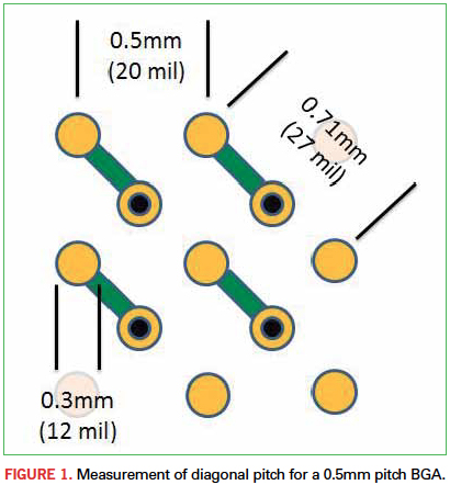
IPC-7095B classifies 0.8mm and smaller pitch as fine-pitch.1 It really starts to get complicated at around that point. For example, take a 0.5mm pitch BGA. When looking to put a via between the pads, the diagonal pitch is the critical measurement. In this case, it’s 0.71mm (17 mils). It might immediately seem like that’s plenty of room for a 6 mil via, but upon closer examination, not so much (Figure 1).
IPC states that a 0.5mm pitch BGA will have a nominal pad diameter of 0.3mm. It should be a non-solder mask defined pad, which will add about 0.07mm to the pad diameter. That gives 0.44mm total pad diameter. The radius is 0.22mm (8 mils). Take that out of the 0.35mm (14 mils) there is to work with and it doesn’t leave a lot of room.
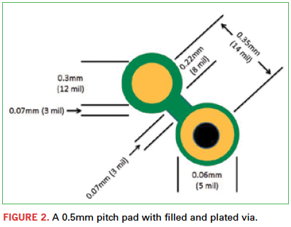
If the fabricator can build 3 mil lines and spaces, the result will be enough room for a 0.06mm (5 mil) via, including annular ring. That’s not much space. Most designers would at that point seriously consider putting the via in the land pad and having it filled and plated over (Figure 2). You can’t leave the via open or unplated. It will cost more, but at these geometries, it’s your only viable option.
References
1. IPC-7095B, “Design and Assembly Process Implementation for BGAs,” March 2008.
Duane Benson is marketing manager at Screaming Circuits (screamingcircuits.com); This email address is being protected from spambots. You need JavaScript enabled to view it..