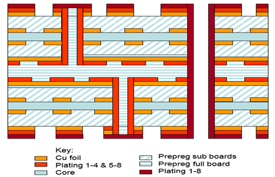
Higher layer count boards with mechanically drilled blind or buried vias may be built separately, then laminated together.
Sequential lamination is a fundamental manufacturing technique in an era of modern PCB fabrication and is a concept that must be especially understood when manufacturing high-density interconnect (HDI) PCBs with blind and buried vias.
Fabricators collaborate closely with designers to prepare their Gerber, ODB++ or IPC-2581 data - the input data for PCB manufacturing. This collaboration ensures that designs are equipped (to varying degrees) with clear, detailed instructions from the outset. For designers and design engineers, this means defining the stackup with all the requirements related to impedance control and sequential lamination.
Sequential lamination is one of the processes used to form mechanically drilled blind or buried vias. In this process, a PCB is built up layer by layer, inserting a dielectric layer between a layer of copper and an already-laminated sub-composite. HDI PCBs undergo this process when different combinations of layers and via structure types are required. Figure 1 shows an 8-layer sequential build, constructed as two separate 4-layer sections and then laminated to make an 8-layer circuit board.

Figure 1. The manufacture of an 8-layer sequential build, which in this case is constructed as two separate 4-layer units and then laminated together.
Basic Manufacturing Steps
The basic manufacturing steps listed below outline the processes involved in making a sequential build.
Sub board (layers 1-4):
- Process the core for layers 2 and 3 per standard process
- Laminate the core to outer layer foils (layers 1 and 4) with prepreg
- Drill holes for 1-4 blind vias
- Image layer 4
- Electroplate the board by putting copper into vias and pattern plates of layer 4 while layer 1 is a panel plate. (Panel plate means the copper foil becomes completely covered with electrolytic copper over 100% of its surface. Layer 4 uses a standard process for outer layers.)
- Etch layer 4 to form a finished circuit pattern.
Sub board (layers 5-8):
- Process the core for layers 5 and 6 per standard process
- Laminate to the outer layer foils for 5 and 8 with prepreg
- Drill holes for 5-8 blind vias
- Image layer 5
- Electroplate the board to put copper into the vias and pattern plates of layer 5 while layer 8 is a panel plate
- Etch layer 5 to form finished circuit pattern.
Complete board 1-8:
- Laminate the sub board 1-4 to sub board 5-8 using two layers of prepreg. (The resin from the prepreg will flow into vias in both sub boards during the lamination process. Two layers help to promote adhesion.)
- Drill holes 1-8
- Image layer 1 and 8
- Electroplate copper in vias 1-8, and standard pattern plate layers 1 and 8.
- Etch layers 1 and 8 to create the finished circuit pattern.
Design Considerations
Designers must consider how well the laminating prepreg flows into the vias in the sub board. The answer depends on resin content and sub board thickness. This is important to understand when determining whether the blind vias will have a copper cap.
The copper thickness on layers 1 and 8 is much thicker than normal due to a panel plate followed by a pattern plate. This limits circuit density.
Layers 4 and 5 have been electroplated, so the copper thickness is higher than that of a standard inner layer. This limits the ability to create fine features, and impedances will be more variable due to the plating process.
Copper Plating
Fabricators often adjust copper thickness to optimize the final product. For instance, they may use thinner copper for layers 1 and 8 or apply a copper reduction process after the final lamination cycle before pattern plate. These adjustments improve etching yield and design accuracy.
Understanding the suppliers’ process and the final copper thickness is critical because this dictates the minimum copper features that can be used in the design.
Akber Roy is chief executive of Rush PCB Inc., a printed circuit design, fabrication and assembly company (rushpcb.com); This email address is being protected from spambots. You need JavaScript enabled to view it..


