Tips and tricks for applications of all speeds, from 1MHz to gigabit level.
How do you know a high-speed design application from an ordinary one? What qualifies as high speed and when does design rigor need ramping?
With CAD tools available to help enforce design rules and the internet at one’s fingertips, PCB designers may implement “best practice” techniques without truly understanding their importance. They may also be missing some less common, powerful and effective techniques as well.
Here we target a broad range of designers and discuss the gamut of lower-speed designs up to gigabit-level speeds. We cover board-level tips and tricks and explain why these tips are important and the nature of the physics behind them. Whether you’re designing with simple I2C or gigabit ethernet, there’s something to be gained by considering even the simplest additions to a design.
Throughout, we explore the common themes throughout all speed applications and the best practices that could extend beyond board-level traces and planes.
Let’s start on the slower end and work our way up.
Low-Medium Speeds (1MHz to 100Mhz)
A competent PCB designer understands the relationship that clock and data frequencies have with a PCB’s physical characteristics, which includes when to increase design rigor. Simple serial interfaces (including single-ended and differential) can produce signal integrity issues if laid out incorrectly, so it’s important to understand the fundamentals of signal integrity, even at these lower speeds.
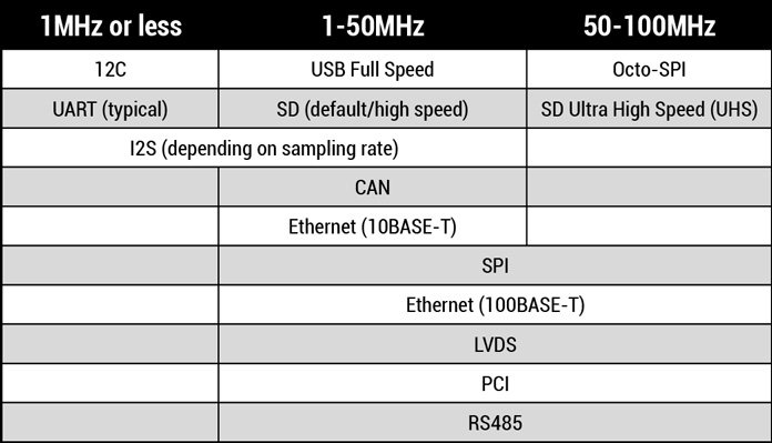
Table 1 features a list of common, industry-standard interfaces that warrant special consideration when performing PCB layout. Note that the clock or bus frequency is what we are looking at here, not necessarily the data rate. The table should indicate where a given design sensitivity might sit concerning these rising and falling edges for lower speeds.
Table 1. Industry-Standard Interfaces for Low-Medium Speeds
Some of the protocols described have good protocol-layer protection and can help improve data integrity (not necessarily signal integrity). CAN is a good example of this, given its failure detection mechanisms.
But let’s look at some of the physical signal integrity issues we might encounter at these lower speeds.
Transmission line effects and propagation delays. For circuit boards including a serial or parallel bus, there is a typical minimum speed (threshold frequency) at which a designer should consider transmission line effects such as reflections, EMI crosstalk and other issues, based on the physical length of the signal path (and a few other things). A widely accepted general rule of thumb is 1/10th of the signal wavelength. Let’s explore that a bit.
Consider the equation
λ = wv / f
where signal wavelength (λ) = signal propagation speed (wv or wave velocity) / frequency (f)
On a PCB, propagation speed is impacted by many things, including parasitic capacitances, impedance mismatches and reflections. But assuming our example contains a well laid-out circuit with minimal issues, the dielectric material effect can be approximated by:
wv = c / √(ε)
where propagation speed (wv) = speed of light (c) / square root of the relative permittivity of FR-4 dielectric material (around 4.5).
This equates to
wv = 3x10⁸m/s / √(4.5) = 1.42x10⁸m/s.
Let’s say we’re staying within a rather large, 10″x10″ PCB design. Consider 20cm (~8″) as a typical trace length of an I2C or UART bus. If we’re estimating the frequency associated with a 1/10th wavelength, then we end up with:
λ = wv / (f*10) → f = wv / (λ*10)
f = (1.42x10⁸m/s / 10*0.2m) = 71MHz
Figure 1 shows a design containing an I2C bus and a total signal length of over 17″. A designer might run a sanity check on this to make sure they’re still within a reasonable margin of seeing reflections and crosstalk.
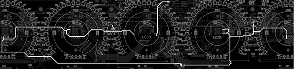
Figure 1. A circuit board design highlighting the “SCK” signal. Calculating frequency limitations for I2C bus stretching over 17" (f = (1.42x10⁸m/s / 10*0.43m) = 33MHz)). This is much higher than the expected data frequency, which may be up to 1MHz.
These 33MHz and 71MHz estimated threshold values fall within our 1-100MHz table including SPI, SD and RS485 applications operating at higher speeds and are well out of reach from slower protocols such as I2C. As pointed out in the walkthrough above, other parameters can impact propagation speeds and greatly impact this threshold frequency if best practice is not followed. That includes impedance matching and some other tips included in this article.
Implementing the following design choices to applications, including the slower speeds (1-50MHz), can help keep propagation delays to a minimum as well as avoid crosstalk and typical EMI issues:
- Using the “star” topology in an I2C application (and slower SPI speeds) is a myth and shouldn’t have any major impact on signal integrity, as shown in the calculations above. If the bus isn’t operating above the 50MHz range, then bus reflections likely won’t occur. At some point, it does matter, and you’ll want to avoid a “star” topology when laying out a communication interface. It’s better to “snake” a bus around a PCB starting with the master or host at one end and the slave devices connected along the path rather than branching out in many different locations (Figure 2).
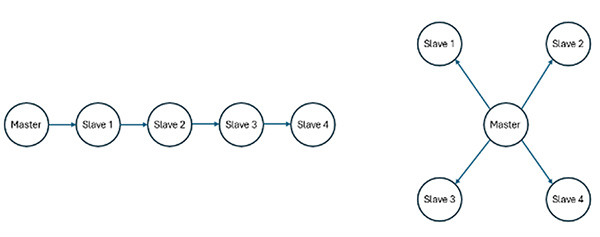
Figure 2. Daisy-chain (left) and star (right) topologies.
- Routing traces alongside a PCB edge increases the chances of EMI susceptibility from nearby, off-board radiators. Keep buses protected and if needed, establish a grounding barrier with vias to help keep EMI off board edges (Figure 3).
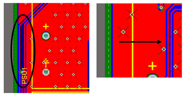
Figure 3. An example of an EMI-sensitive design containing a signal routed on the outer edge of a PCB. This should be moved off of the board edge and routed through the polygon pour.
- Limit the amount of vias used when routing signals from one layer to the next. In this speed range, it’s best to limit the amount of vias (per signal) to no more than three.
- Pull-up and pull-down resistors typically have a positive effect on signals and help accelerate rise times or fall times while preventing stray signals, though depending on the driving circuit, they may require some tuning. This improved propagation timing helps keep delays to a minimum and out of the danger zone with respect to transmission line effects (Figure 4). The value of the pull-up/pull-down resistor is usually specific to the signal and its conditions, and often is recommended by a chip manufacturer or even an IEEE standard.
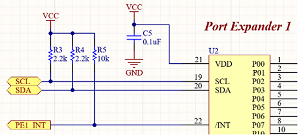
Figure 4. An example of a port expander’s I2C bus containing a very typical 2.2kΩ pull-up resistance, while its interrupt signal contains another very standard 10kΩ pull-up resistance.
- For applications in the 50-100MHz domain that may experience some transmission line reflections, it’s common to slow down the driving signal and dampen the ringing with the placement of a series resistor (Figure 5). This can be done for longer SPI bus layouts where you place a resistor (typically 22-33Ω, which typically helps achieve a 50Ω target line impedance) in line with each source. Place these resistors near the MOSI, SCLK and CS pins at the master end and the MISO pin at each slave’s end.
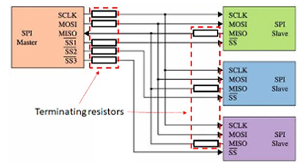
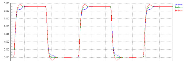
Figure 5. A schematic description of SPI bus termination resistors (top) and the impact of source termination resistors on a high-speed signal waveform (bottom)
High Speeds (100MHz to 1Ghz)
Now that we’ve discussed some of the basic details to consider at lower speeds, let’s kick it up a notch.
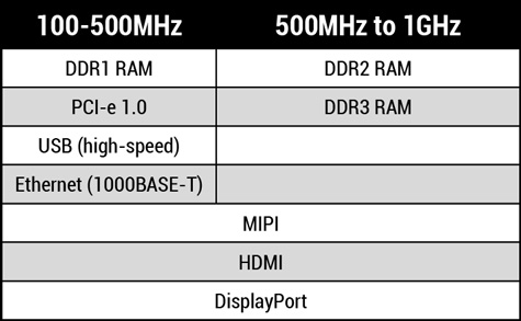
Table 2 is another list of common, industry-standard interfaces that require closer consideration during PCB layout for higher speeds. Here we will focus a bit more on rise and fall time considerations.
Table 2. Industry-Standard Interfaces for Medium-High Speeds
With clock and data frequencies operating above 100MHz, a designer must pay close attention to the relationship between rise time and frequency (Figure 6).
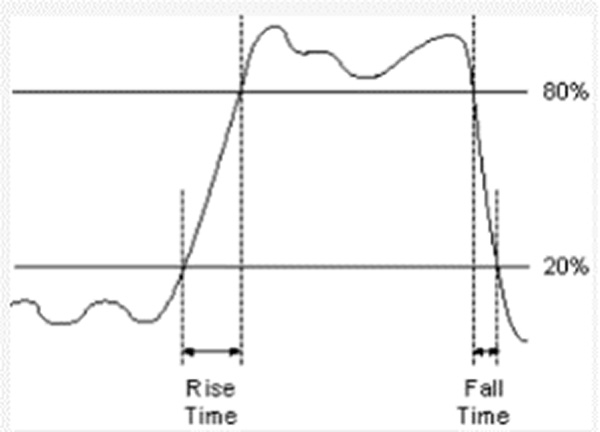
Figure 6. Rise and fall time visual indication of a signal.
In general, a rise or fall time is defined as the transitional period of a signal’s edge, typically making up 10-90% of the edge, and ruling out the first and final 10% zones due to anomalies and differences seen in switching patterns from one device to the next (some have slow roll-off, etc.). A circuit can never support zero rise or fall time; it’s impossible. This transition will always have some sort of delay. But the key is that it must support fast enough transitions to not lose valuable information at higher frequencies.
Going too fast may cause undesired effects as well. So, these rise and fall times must be characterized and controlled.
A good rule of thumb here when relating expected rise or fall times to frequency is:
TR/F = 1 / (f * π)
For a frequency of 100MHz, a designer should expect (or strive for) a rise or fall time on the order of 3-4ns. 500MHz should be more in the 0.5-1ns range. We can use this to determine what an acceptable trace length would be for a given signal, and we’ll see here that they are proportional to each other.
Another general rule of thumb: the critical or maximum trace length for a given signal should permit a propagation time of no longer than half the rise or fall time. This can be written as
Critical trace length = wv * ½ TR/F
Let’s apply this to an example. Say that we have a 100MHz signal, which is estimated to have around a 3ns rise time. Incorporating our previously calculated propagation speed of 1.42x10⁸m/s, we get the following
Critical trace length = (1.42x10⁸m/s * 3x10⁻⁹s) / 2 = 21cm (~8″)
Applying this same formula to something operating at 500MHz produces a much shorter critical trace length:
Critical trace length = (1.42x10⁸m/s * 0.6x10⁻⁹s) / 2 = 4cm (~1.6″)
These calculations assume (as was done before) that our propagation delays are minimal. Any negative impacts to this propagation timing or the rise and fall times (such as parasitic capacitance, inductance due to ground bounce, reflections, etc.) greatly impact this critical length, and it’s why we must incorporate more rigorous tips/tricks with the PCB layout.
Here is a list of higher-speed tips and tricks for the 100MHz to 1GHz range:
- At these speeds, a clean power source needs to be used for all digital ICs involved. This includes using higher-quality ceramic capacitors like MLCCs that are good at reducing local EMI, decoupling noise and reducing voltage ripples. Use linear regulators whenever possible, but if incorporating a switching supply, make sure to source a quality, low-noise supply and implement a good practice layout for the switching paths to minimize board parasitics and transients (Figure 7). Also, be generous with ferrite beads, especially if a power source is coming from an off-board source.
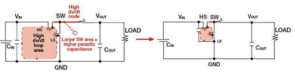
Figure 7. Effects of a larger SW area/trace length, resulting in more parasitic capacitance and unstable regulation.
- Impedance control greatly helps reduce reflections, crosstalk and inductive coupling. Impedance control involves many factors, including PCB stackup materials and their dielectric constants, trace width, thickness and spacing. PCB materials and controlled-build specifications become much more crucial beyond 1Ghz, as we’ll see in the next section. Length tuning is part of this impedance-matching activity and ensures minimal differences in propagation delay between signal pairs. Serpentine routing on differential pairs is the ideal form of length tuning for interfaces that contain several lanes of differential pairs (all of which need to be tuned together) (Figure 8).
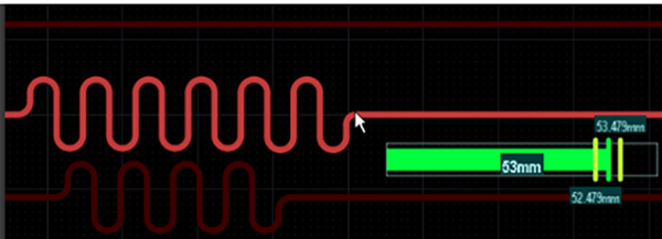
Figure 8. An example of serpentine length tuning.
- The well-known “3W” rule for impedance control states that, to minimize crosstalk between two traces, the designer should permit a minimum spacing between the differential pairs equal to three times the width of the track (measured from center to center of the trace) (Figure 9).
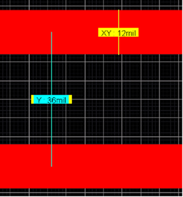
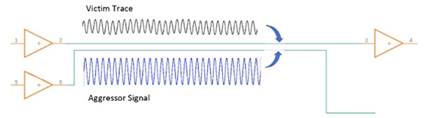
Figure 9. An example of a differential pair including 12-mil traces, separated by three times the width of the track (36 mils).
- Implement shielding wherever possible, including the use of ground planes, stitched vias and off-board connections.
- Layer stackup is important, especially if internal layers are used for routing sensitive signals. Ground planes can be used as shields for applications involving several layers and can also be used to minimize crosstalk by maintaining sufficient spacing between signals and planes. A designer can implement “plane pairing,” which is similar to having adjacent power planes and signal planes reduce current loops and lower EMI radiation.
- Avoid using vias on data and clock signals in general. Using vias on high-speed signals extends their length and exposes them to innerlayers, increasing opportunities for inductive coupling and EMI impacts. If vias must be used, avoid stubs (use blind and buried vias) as these can cause reflections.
- Avoid routing sensitive signals across two different planes or over top of other (unshielded) nearby signals on different layers (Figure 10). If you must, route the traces such that they cross in a perpendicular direction rather than parallel.
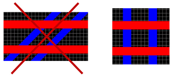
Figure 10. Route a sensitive signal overtop its reference ground and not across other ground reference planes (top), and route high-speed signals in a more perpendicular fashion with respect to traces on other layers (bottom).
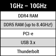
Super Speeds (1Ghz to 10GHz)
Finally, we arrive at super speeds. These are the fast digital interfaces used today and require the utmost attention to detail during PCB layout. Rise and fall times will be in the picoseconds so the associated trace lengths and EMI protections are critical.
At this level, it is crucial to understand the fabrication and layer stackup specifications, as well as communicate those to the PCB vendor for DfM feedback.
Table 3. Industry-Standard Interfaces for High-Super Speeds
Here are some considerations for these super-speed applications:
- Use PCB materials with a low dielectric constant to minimize timing delays. Higher-performance materials such as PTFE may drive cost but provide lower losses at higher frequencies. Work with your PCB vendor on recommended materials and cost/benefit tradeoffs and utilize layer stackup tools.
- Understand when to use microstrip (outer layers) and stripline (innerlayers) for routing data and clock signals, and how to configure ground planes associated with the signals. Impedance control will be different for outer layers versus innerlayers and should be calculated using CAD. Also, be sure to understand the source and load characteristics of these traces.
- Be generous with ground planes in designs featuring several layers. Each digital interface may require its own designated innerlayer with ground planes above and below to shield from EMI as well as provide minimized ground loops and clean return paths. Try to keep all byte lanes on the same layer if possible, but if needed, then alternate the byte lanes across two different layers. Figure 11 shows several layers containing high-speed signals. Some layers are paired with others and are part of the same bus, such as orange and purple.
Figure 11. An example of multiple high-speed lanes routed on several inner layers, some of which are part of the same bus.
- While adding layers to a design, keep an eye on layer stackup symmetry to provide mechanical stability. This includes evenly distributed copper across the stackup, which should prevent warping.
- When routing clock and data traces, maintain the critical length rule described in the previous section. It’s also ideal to avoid any corners at all (even 45° bends), and keep all traces serpentine if possible. Right angle traces can act as antennas and cause radiation due to added capacitance in the corner. Minimize this by rounding off the corners of sensitive signals (Figure 12).
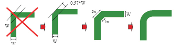
Figure 12. An indication of poor and good right-angle bends
- High frequency typically translates to high heat. Make sure to plan on thermal management and proper heat dissipation including thermal vias, heat sinks and polygon pours.
- Simulate and test your designs as much as possible. This includes eye diagrams, thermal management, insertion/return loss and voltage ripple on associated power rails. Eye diagrams (which can be both modeled and tested) provide a great metric for jitter and timing as well as ensuring that data and clock signals fall within the acceptable limits of a standard (Figure 13). Thermal management can typically be modeled and reveal potential hotspots, but should be measured on prototype designs. S-parameters are used to characterize high-frequency behavior and include analysis of expected losses and transmission efficiencies. Depending on the manufacturer, low-noise power supplies can typically simulate voltage ripple and loading effects.
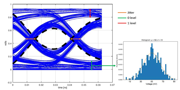
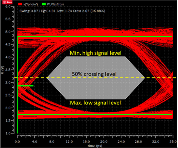
Figure 13. An eye diagram indicating jitter and normal distribution of 0-level (top), and a demonstration of how to interpret an eye diagram and ensure that all signal traces stay out of the mask area (bottom).
- Finally, it is always ideal to build a good relationship with the board supplier and ensure that proper DfM feedback is provided, as well as guidance in many aspects such as material selection, clearances and tolerances, and layer stackup. Begin by basing your design on vendor design rules. Don’t wait to check to learn you’re following a reasonable set of specifications.
Ultimately, it helps to know when to incorporate the proper rigor for PCB layout and it’s important to understand the physics involved with these widely accepted rules of thumb.
By understanding the fundamentals behind signal integrity at higher frequencies, you’re less likely to end up with a design with reliability problems during both initial board bring-up and system integration. And there will always be a tradeoff between cost and complexity.
By consulting with your PCB vendor regularly and performing due diligence upfront, a designer can find an ideal balance that is both cost effective and high performing.
Andrew Gonzales is VP of engineering at San Francisco Circuits (sfcircuits.com); This email address is being protected from spambots. You need JavaScript enabled to view it.. Jason Metzner is a senior systems engineer at Arthrex (arthrex.com); This email address is being protected from spambots. You need JavaScript enabled to view it..


