Higher signaling speeds require better signal integrity, thus designing multi-GHz or multi-Gb boards has to involve better knowledge and tools than ever.
Impedance measurements. Traditionally, impedance is measured by time domain reflectometry (TDR) on test coupons. Test coupons are manufactured on the same panels as the actual PCBs, and contain the same controlled-impedance traces (same width, same layer). Reason: It is easier to probe traces on a test coupon than on an actual, dense PCB.
TDR instruments generate a single very short pulse signal, and measure the reflected or arrived signal at the other end of the trace. Based on the TDR result voltage levels, the instrument or user performs some post-processing to get the measured impedance.
To take accurate frequency-dependent impedance measurements, set the TDR instrument to the same rise time as the signal would have on the actual PCB on the appropriate signal trace. (In practice, manufacturers don’t do this, although most TDR instruments have the option to set the rise time. Normally, a manufacturer has its favorite rise time setting and uses it for all measurements.) Some TDR instruments don’t have the option to set rise time; others do. This could lead to measuring impedance on a different frequency than it should be, and could result in a measurement error (Figure 8). The error is relative to the requirement, not an absolute value to the ideal impedance, since in reality, both the impedance requirement and the measurement are frequency-dependent.10
One way to do single frequency-point impedance measurement is to use a vector network analyzer (VNA) instead of a TDR. There are simple programs based on analytical equations, but they are outside of the scope of this article, as the calculation error can be 5 to 50%. Instead, we are focusing on field-solver programs, for which the only possible inaccuracies are the not-infinite mesh density, the wrong frequency, simplified modelling and improper usage. (For most programs, the software developers internally set mesh density.)
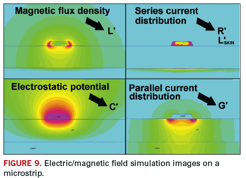
Field-solvers divide the geometry (2-D cross-section) into small pieces (nodes) – a process called meshing – and then solve the Maxwell’s differential equations in all of them to determine electrostatic and magnetic fields and current distribution (Figure 9).
Next, as post-processing on these fields and currents, they determine the RLGC per-unit-length parameters. Finally, they calculate impedance as described. Typically, they calculate w –> Z0 directly, and if the opposite way of calculation is needed, then they iterate until they reach the desired characteristic impedance within a user-specified tolerance (0.1 to 5%). Some samples:
Polar Instruments Si8000. This is the industry standard frequency-independent impedance calculator. It calculates everything on 2 GHz. The Dk value must be pre-compensated to the signal’s frequency or to a suitable value. (For computer boards, 2 GHz is sufficient.) It calculates both width –> impedance and impedance –> width.
Polar Instruments Si9000. This is the extended version of the Si8000, with some frequency-dependent parameter calculations. It only calculates width –> impedance in a frequency-dependent form, and impedance –> width only in a frequency-independent way, or with manual iterations. For the former, it compensates (as an option) for Dk over frequency.
Polar Instruments Speedstack. A stackup builder, it uses Si8000 or Si9000 for impedance calculations, but its material library does not support frequency-dependent Dk specifications. So, in case of using together with Si9000, we need to override Dk, impedance and width values.
TNT-MMTL (open source; available at Sourceforge). Developed by the Mayo Clinic Special Purpose Processor Development Group, it can do both ways w –> Z0, and w –> Z0. In comparison with the Polar Si8000 in a few different tests, I calculated a maximum 2% difference for coated microstrips, and less than 1% for stripline structures. This is frequency-independent.11
Appcad RLGC. This program calculates the transmission line RLGC parameters, and the user has to calculate the impedance from them. This is frequency-dependent.12
General-purpose 2-D field-solvers. Examples include Ansoft Q3D Extractor, FEMM (FiniteElementMagnetics, open source). These programs provide the opportunity to set every simulation parameter, so they can be used on any levels of accuracy. We can draw any arbitrary-shaped cross-sections, and model multiple material platings on the conductors. They only work in the width (geometry) –> impedance way. They are normally frequency-dependent. The simulation setup may take several hours, since we have to hand-draw the geometry, do mesh seeding at critical areas and specify material parameters, perform simulations, and post-processing. After several simulations, we can get the RLGC parameters or matrices to use to calculate impedance.13
Frequency-Dependent Impedance Control Drawbacks There are certain problems with frequency-dependent impedance control. For one, at the time of this writing, there was no available accurate, fast method/software to calculate trace width from impedance requirement on a user-specified frequency.
Second, PCB manufacturers do not perform frequency-dependent impedance measurements. They often say they do, but usually they have their choice of a specific signal rise time, yet it is fixed for all their measurements. The basic principles of TDR impedance measurements are frequency-independent. There is no method under which TDR could discern the test coupon impedance on a given frequency, since the TDR signal also is a wideband signal. One way could be to set the TDR test signal at a similar frequency spectrum as the digital signal, which – simplified – means setting the same rise time on the TDR as the digital signal. But it is not proven why it would be more accurate, and the theory remains under study.10
Third, there is no exact method found for time domain to frequency domain signal conversion. For digital signals, it is hard to select a single frequency, since they are wideband signals and defined in time domain. There could be several user-based choices (knee frequency, clock frequency, mean of band, etc.) to pick up as a part of the signal’s frequency spectrum. So, the selection leads to more inaccuracies.
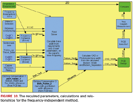
Frequency-Independent Impedance Control This is a subset of the previously described frequency-dependent method. On a certain level, it still must be frequency-dependent: As a minimum, we must compensate for the frequency dependence of the dielectric constant, since it usually is provided on a very low frequency (1 MHz). Before putting material Dk and Df information into the calculator or its library, compensate for them to a suitable frequency (e.g., for computer boards, 2 GHz is sufficient) (Figure 10).
The method is the same as described in the frequency-dependent calculation, with the following differences:
The field-solver does not need the Df data, but the Dk compensation still does.
The TDR measurements can be done with the usual constant rise time.
Dk values can be set into a material library once, and don’t have to be overriden at every calculation, based on the signal’s frequency.
Available software provides a quick way for the impedance –> width calculation required for common product design.
We don’t care about the frequency spectrum of the digital signals in frequency-independent calculations.
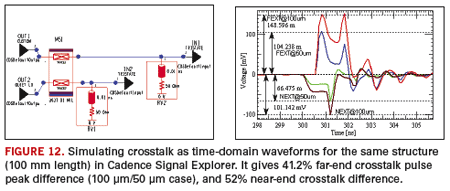
Stackups and Signal Integrity Crosstalk. There is no impedance control without crosstalk control. Maybe some do impedance control when not taking crosstalk into account, but the boards will behave unpredictably. If we change a stackup to achieve the impedance requirement, then the crosstalk levels also change.
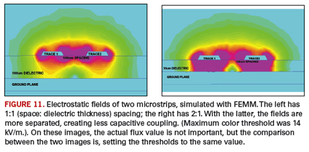
Crosstalk between traces on the same layer. Among several parameters, the trace separation versus dielectric thickness ratio (and not the width versus separation ratio) has a significant effect on crosstalk noise (Figure 11). If the dielectric material (thickness) is changed in the stackup, then the crosstalk levels between the traces change too. If thickness increases but trace-separation remains the same (between traces on the same layer), crosstalk increases. So, if it must be changed on a board post-prototype, only decrease the thicknesses (between signal layer and ground/reference plane); never increase them. Increasing the dielectric thickness will increase the ground return current areas and their overlapping (different signals) area. It also increases the mutual inductance and mutual capacitance. Crosstalk can be traced to mutual inductances and capacitances between traces, so they must remain low. A poor but widespread practice is to allow different fabricators to change the stackup based on their material stock. Material change usually means dielectric thickness change, which changes the crosstalk levels. Typically, those involved are too ill-informed to know they are changing the crosstalk levels too. To avoid problems, a design or signal integrity engineer must be involved in approving new stackups for existing boards, and they have to understand the effects. Otherwise, poor yields or field failures will occur at random.
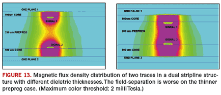
Crosstalk between traces on different layers (dual striplines). Since the two signal layers reside in each other’s magnetic and electrostatic fields (between the same two reference planes), there is a lot of parasitic inductance and capacitance between the traces. A usual technique is to perpendicularly (90°) route the signals on the two layers, avoiding long coupled segments between them. The crosstalk levels (mutual L, C) are higher for longer parallel trace segments. For complex digital boards, it usually is impossible to maintain 90° routing. Do not use dual striplines. (Use more ground planes.) Try to minimize the overlapping areas of the magnetic flux and electrostatic fields (Figure 13) on the two layers to minimize crosstalk. This can be accomplished by putting the signal layers closer to the two different reference planes, and farther from each other. Poor industry practice (changing stackups without approval by hardware or signal integrity engineers) has the same effect on this type of crosstalk as was described in the previous section: changing crosstalk levels without control or attention (indeterminate behavior).
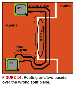
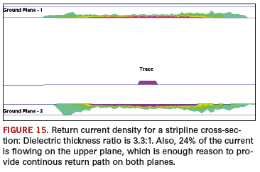
Crosstalk caused by return current discontinuities. When the return currents of multiple traces are forced away from their natural path to a plane-split edge, they induce noise currents into each other’s signals. Since the return current in these cases is not flowing underneath the traces but with a few millimeters offset, they create a current loop. One branch of the loop is the signal (signal current) and the other is the return current (Figure 14). For plane discontinuities, these loops of different signals overlap, and they effectively create a single-turn transformer between the signals, which creates strong crosstalk. The obvious response is to route all signals only above continous planes. Both planes must be continous for striplines, since the return currents flow in both planes (Figure 15).
For stripline structures, provide the current return path in both planes, not only in the closer one, since the return current has its natural path in both planes. For dual striplines, both signal layers have return currents in both planes.
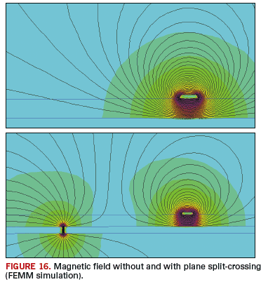
Layer change without stitching vias (or stitching/decoupling capacitors) also belongs to this problem group, since after pulling the signal through the stackup, we also have to provide the return current path through the stackup to the appropriate planes (between the reference planes of the start and the destination signal layers). Impedance discontinuities. The trace impedance will be the same as the calculated value if there is a path provided in (both) the reference plane(s) where the return current can flow. If we cut its way (plane split), or the signal’s driver or receiver chip’s ground pin has no short (AC) connection to the reference plane(s), or there are voids on the plane (antipads), then the return current is forced away from its natuaral path (right underneath the signal trace with a specific current distribution shape), and the calculated impedance is no longer valid. It is a simplification to say the impedance is defined by the PCB cross-section geometry. In reality, it is defined by the shape of the distributed currents in both the trace and reference planes, and by the shape of the magnetic and electrostatic fields. These field shapes are guided by the geometry.
For example, a 100 µm wide microstrip trace over a 100 µm dielectric has an impedance on 1 GHz of 69.5Ω (based on FEMM RLGC simulation), but when the trace has to cross a plane split and go above the wrong plane in parallel to the split edge at a distance of 9 mm for awhile, then the impedance will be 158.9Ω, a huge difference (Figure 16). The reason is the modified current return path inside the reference planes, which increases ground path inductance. Another reason is that the trace capacitance (electrostatic field) now has to go through the plane split too, so the C parameter is decreased. If there is a big void on a reference plane, it creates the same problem: The return current cannot jump to the next plane for that part of the signal path, but only flows on continuous copper. In some cases (not between analog and noisy-digital grounds), this return current path can be provided by using stitching capacitors over the split.
The two main reasons why discontinuities are bad are 1) if 50Ω are needed and 150Ω are obtained, then obviously the impedance requirements are not met, and 2) discontinuities also significantly increase crosstalk and EMI.
3-D discontinuities. Via transitions, connectors and IC package pins create 3-D discontinuities that only can be modeled by 3-D electromagnetic simulators (e.g., Agilent Momentum, Ansoft HFSS, CST Microwave Studio, Cray-LC). These 3-D discontinuities create impedance deviation from the simply calculated values, and introduce parasitic inductances and capacitances into the signal path. The previously described discontinuities also are 3-D, but are so flat, they can be handled as 2-D discontinuities.
Conclusions Not only must cross-section parameters be taken into account, but also other layers in the stackup, reference plane discontinuities, the used signals, the pattern on the copper layers, and so on. Because higher signaling speeds require better signal integrity, impedance control for today’s multi-GHz or multi-Gb boards has to involve more knowledge (PCB manufacturing technologies, high-frequency measurements, signal integrity, electromagnetism, material science) and more sophisticated tools than was necessary even a few years ago. One part of maintaining good signal integrity is to control impedances within a tight range.
For a quick way to perform everyday calculations for design, use a frequency-independent method for simplicity, with a few parameters considered on an average or usual constant signaling frequency. For computer motherboard designs, 2 GHz seems to give the best accuracy. The fully frequency-dependent method is not completely developed, especially not from the design point of view. It may be used for analysis for verifying the impedances. PCD&F
References 10. Simberian Inc., “Micro-strip Line Characteristic Impedance and TDR,” application note #2009_04, April 2009. 11. Mayo Clinic Special Purpose Processor Development Group, TNT MMTL freeware field solver program, http://mmtl.sourceforge.net/. 12. Applied Simulation Technology (Apsim), AppCAD RLGC, http://apsimtech.com/. 13. The field-simulations in this document were prepared in the Finite Element Method Magnetics (FEMM) freeware/opensource 2-D fieldsolver program (http://femm. foster-miller.net).
Istvan Nagy is hardware design engineer at Concurrent Technologies (cct.co.uk); This email address is being protected from spambots. You need JavaScript enabled to view it..
The right impedance ensures against additional SI or EMI issues.
A well-designed power distribution network (PDN) must have low impedance on the delivery path. The question is, How “low” is enough so that a PDN can deliver sufficient power supply for ICs to work properly? To answer this, we first need to define the impedance so that a PDN can be mathematically represented.
Suppose a PDN to be a linear network with named nodes and branches, and current flowing from VRM through PDN to ICs. The impedance at any location of a PDN can be defined as
The impedance here is the ratio of actual node voltage change to the total dynamic current drawn by ICs at any frequency point. If the total current is normalized as 1, the node voltage at any location gives the impedance at that node. At a given frequency, when x and y are the coordinates of IC power supply pins, the impedance would be the one seen by an IC component to the PDN, which is what board or system designers are interested in, and needs to be minimized. Figure 1 illustrates a good PDN as it appears in the frequency domain.
It is important to emphasize the PDN impedance is defined in frequency domain. Then, how do we use it in a digital design, which works with transient signals in time domain?
Time domain considerations. Considering the power supply for an IC needs to be steady at a required DC level, and the IC can tolerate certain variation of DC voltage (ripple and sag), the DC voltage level and the tolerance give the variation range of power supply. Since the voltage changes in the time domain consist of frequency components at all frequencies, the goal of a PDN design can be described by the minimum range of voltage changes, and maximum current drawn by ICs. This is what we call the target impedance Zt
Here, the supply voltage and allowed ripples (in percentage) give the power supply budget, and the current is the worst transient current drawn by ICs connecting to PDN. Because voltage ripples and the worst transient current can happen at any frequency, this makes the target impedance independent of frequency. In practice, the target impedance, which is effective at all frequencies, is neither achievable nor necessary due to the limited switching speed of a physical IC.
Because the voltage ripples are caused by the combination of the switching currents of all ICs, which a PDN needs to provide power to, the term “current” in Eq. 2 represents actually the total allowable current to switch at the same time. It does not identify when and where individual switching currents occur. From this point, the target impedance in (2) is rather pessimistic; a design meeting the target impedance of (2) may not be an efficient one.
In high-speed digital designs, chips switch their states in sequence. Therefore, all switching current has its profile in time domain. When switching current with a certain profile happens, it means a time variation current source is applied to a PDN at one or several ports (IC power pins). This current induces voltage drops across PDN, which reveals the actual voltage a chip will get during its state changes.
The last question on IC current would be where a PDN designer can obtain switching current profiles. As discussed, the switching current represents the dynamic power consumption on chip, which consists of core and I/Os. Considering the simulation tools for board or package have no access to the IC database, and the chip structure is generally beyond the scale of board/package tools’ solving capacity, the best approach for getting accurate switching current profiles is to contact IC manufacturers that own power analysis tools and measurement equipment for chips. Fortunately, IC manufacturers are willing to provide such information to system designers.
One last caveat: This discussion about PDN impedance assumes a power delivery path ends at the BGA of a component mounting on a printed circuit board, and IC current is drawn directly at BGAs. In reality, the actual component on board includes chip and package, which introduce additional inductance and capacitance to be resonant with the rest of the PDN impedance. Package parasitics and on-die capacitance can be included in PDN if both models are available. However, the new PDN impedance becomes “component-dependent.” If a component is replaced by another, the impedance of the entire PDN needs to be reanalyzed. A better solution is to equip PI tools with user-preferred options about package and chip effects.
Although power integrity is relatively a new term in high-speed digital design and analysis, its concept has been used in designs for many years. The goal of power integrity is to have PDN provide sufficient power supply to ICs efficiently, without introducing additional SI or EMI problems. The important means to designing a good PDN is to make PDN impedance below predefined target impedance. PCD&F
Dr. Zhen Mu is product market manager at Mentor Graphics (mentor.com).
Recent horror stories remind us that designers really need to know it all.
A recent blog on the Circuits Assembly websitegot me going on one of my pet topics. This will come as no surprise to those of you who know me, but once I overcome inertia and a latent proclivity for procrastination, I usually have to take a nap, thanks to all the effort of overcoming said inertia and procrastination.
But not this time.
This time the subject close to my heart is design for manufacture. The blog, written by regular contributor Duane Benson of Screaming Circuits, is titled “Another Land Pattern Mixup." It is just so difficult to understand how, after all this time, we still cannot get right certain fundamental things between design and manufacturing.
Now I won’t pretend to know the particulars here. There may have been a mistake when the part was created; the part number may have changed somewhere along the line, or someone at the CAM station may have screwed up. I don’t know. But I do know that here is a board that has a land pattern that will not accommodate the component supposed to go in the circuit.
Duane also shows an example of what looks like a jumper strip that is probably a metric part, but at first glance, it appears the designer used imperial dimensions. It probably would work if there were only a few pins, but over the length of 11 pins, the conversion round off or tolerance means the part won’t fit into the board. At first blush, we naturally would say the designer screwed up. But what if somewhere along the line, purchasing or some other entity substituted a part that “looked the same” to save a penny or two? In many companies, a librarian is responsible for creating the footprints. Sometimes this person is not a designer or does not really understand all the implications of what they are doing. Whatever the cause, there is a preventable problem here.
I’m not going to put all the blame on the designer because the truth is, in many cases, neither side of this issue really understands the fundamentals of the other. Many people in manufacturing really do not understand who the designer is, much less what they really do. The only thing they know about the designer is what they read in the media or see in the Gerber files. And before we go further, I’ll add that, yes, some folks in the media write about design and manufacture and don’t know who or what the designer (or the fabricator, for that matter) is. They may fool some folks, but designers usually can tell the difference between those who have had to find a way to connect those last few traces and those who have not.
When it really gets down to where solder meets laminate, the buck stops at the designer. No matter what the problem is, more than likely whoever designed theboard is going to take the rap. In most cases, that is as it should be. Fabricators and assemblers may not need to know how to design a board, but designers need to know how every aspect of the PCB manufacturing process affects their decisions. One of my drafting gurus told me that, after I finished a drawing, I should stand back, look at the drawing, and ask myself if I could build the part from the information on the paper (yes, paper; it was the 1970s). The catch here is that if you don’t know what happens in the shop, you can’t answer those questions.
Over the past 20 years, PCD&F and Circuits Assembly have published countless articles about DfM. We’ve produced scores of classes at the PCB Design Conferences, and I’d like to think many designers know a lot more about manufacturing than they did before they read those articles or attended those classes. So it boggles my mind that we still see the kinds of problems Duane points out.
I know there are pressures to get the design out now! A host of other issues play into this as well. But what good is a design done quickly, if it has this type of problem? What’s the cost of doing another run of prototypes, both in dollars (or euros or yuan) and time? Every manager and bean-counter should be required to read Duane’s blogs and other horror stories, so they have a better understanding of repercussions of decisions made in the design process.
Having made those claims about our attempts to eliminate DfM problems, I’ll still take some of the blame. Our mission includes educating and bringing the sides together. Evidently we haven’t done a good enough job of that. In the coming months, we’re going to recommit to this mission. But it has to be something in addition to articles and sessions at our shows. Those are important parts of the puzzle, but we need more. Next month, I’ll let you in on what I have in mind.
Until then, stay in touch and, as humorist and author Tom Bodett says, we’ll leave a light on for you. PCD&F
Pete Waddell is design technical editor of PCD&F (pcdandf.com); This email address is being protected from spambots. You need JavaScript enabled to view it..
Merger mania strikes again. Will it play out differently this time?
Just when you thought it was safe, along comes déjà vu all over again!
In so many ways, our industry looks much different as we embark on the second decade of the “new millennium” than it did in the last decade of the past one. Fewer companies are competing, and there is a very different global geographic distribution. Quality and on-time delivery – every company’s means for dramatic improvement a decade ago – are no longer differentiators, as everyone has dramatically improved and performs equally. Technology itself has marched along so quickly that what was “cutting-edge” a decade ago would be considered “commodity” today. But in one way the 1990s are alive and well: Merger mania has once again struck industry boardrooms.
For those who may not remember (or who wisely forgot!), in the mid 1990s a buyout group began a rollup of smaller (albeit what in today’s world would be considered large) companies into what is now Viasystems. On the heels of this business model, and with the encouragement of some of the then-brightest Wall Street analysts who covered our industry, others followed suit. Remember Hadco and Praegitzer? They were caught up in the mania, as was DDI, Altron, Continental Circuits (the Phoenix version), Coretec and a host of much smaller and all-but-forgotten companies.
Like many, I have fond memories of the halcyon ’90s. And I’m not necessarily against mergers; in fact, if someone came along with a boatload of money, I too might sell in the proverbial New York minute. But looking at the carnage, and considering the cost vs. value of those transactions, I have to ask, “What are you guys thinking?!” If the mantra of the ’90s was quality and on-time delivery, the mantra of the new millennium has been “value,” and it takes some stretch to understand how most mergers create value. Early in my corporate career, I was responsible for “business planning,” which included mergers and acquisitions. Being with a Fortune 100 corporation, we sold a lot of businesses that no longer fit with our ever-changing corporate “vision” of businesses – usually selling poorly managed or neglected facilities.
We never seemed to do well buying other companies either. Too often after closing a deal, we would soon find that the culture, capability and claimed strengths of what we had just bought weren’t quite as advertised. More than a few acquired facilities quickly made their way to the list of poorly managed or neglected facilities that were sold! The exceptions were the few cases where the acquired facility filled a specific niche, or where we could shut down the facility and assimilate the business into an existing, better-managed facility. My take from a few years buying and selling was that, once all the dust settled from the deal, rarely was any value gained.
Looking back at the volumes of merger activity, I believe the same was true: little or no real value resulted from all the deals. Surely most companies actively in the hunt for deals are no longer in business. More telling, the capacity footprint is a shadow of its former self, both for the companies involved in those mergers and the industry as a whole.
What is different this time? Instead of the heady, egocentric hype of last decade, this round has been lower key, keeping with the economic mood of the times. In some ways today’s transactions appear more like a hybrid of Jack the Ripper meets Pac Man. But the results appear headed to the same conclusion, which is to say that little, if any real value will result from the (sizable) investments made.
This brings me back to the déjà vu aspect of today’s merger environment. Several of the megadeals have involved the same companies who lost so much the last time they forayed into the M&A world. You would think they would have learned that as attractive as an acquisition may appear, the end-results don’t always warrant the time, talent and treasure initially invested and subsequently required. More to the point, in an industry that has a voracious appetite for investment in technology and the capital equipment to produce it, maybe money can and should be better spent building the competence of a company’s technology franchise in order to build value.
Customers are searching for technology solutions – answers – for the next generation of product. Building value requires being able to invest in and develop technology. Equally, as the equipment used by many in our industry is getting long in the tooth, investing in more, older equipment and infrastructure via an acquisition heightens the risk.
Some may say that merging large companies will increase value by consolidating excess capacity or reducing the unsustainable “desperation” pricing that sometimes results when weaker companies make last-ditch efforts to fill plants. However, if those involved are that weak, they eventually will founder, and the same result achieved with no investment required.
I do hope this time around, these mergers have a happier ending. In each case, hopefully the acquiring company really needs additional capacity and capability, and the corporate culture fits with their needs and actually increases value for all.
But we should keep in mind the companies that survived previous downturns were, and are, ones that regardless of size or location have remained focused on building value by satisfying customer needs. And customers need technology development and solutions for tomorrow’s products. The greatest single value-adding strategy any company can follow is to stick to its knitting and invest in developing the technology and capability to service customers and their markets. PCD&F
Peter Bigelow is president and CEO of IMI (imipcb.com); This email address is being protected from spambots. You need JavaScript enabled to view it.. His column appears monthly.
At the risk of beating the tin drum (and wasn’t that movie painful enough to sit through?) once too often, I will mine (get it?) the Conflict Metals subject one last time.
To recap, Conflict Metals refer to ores extracted from the battle-raged Democratic Republic of Congo, where millions of citizens have died, casualties of a fierce civil war underwritten in part by revenues from contested mining activities.
Following my last two columns, I have heard from various sources who hoped to refine my thinking. One noted that the Congo supplies less than 5% of the world’s tin, suggesting the electronics industry, which as these things go is hardly a major consumer of the metal (some estimates put electronics’ share at 2% of the global consumption), could survive just fine without the DRC as a source. (By the way, tin owns no patent on the issue. The DRC also sits on large deposits of tantalum.)
Second, while the audits proposed by the International Tin Research Institute and other similar-thinking groups (see last month’s Caveat Lector) are a step in the right direction, in some cases they are redundant with existing corporate practice. And reclaimed materials are exempt from the discussion, because, among other reasons, the alternative would be to landfill the disputed metal. As Cookson Electronics president Steve Corbett, one of the few willing to speak on the record, told me, “Customers are not looking for verification on reclaimed materials. And we say, ‘You really don’t want to throw a wet blanket on reclaim, because you want to keep it out of landfills.’ ”
In that sense, even the most intense certification programs are inherently incomplete. While some companies would be able to guarantee there are, in the words of one colorful source, “no Congolese atoms” in their products, there simply is no way for industry as a whole to ensure its products contain no amount of Conflict Metals.
In the US and elsewhere, pending legislation – which one source called “ludicrous” – emits the radioactive notion that through industry pressure, governments can solve the civil war. “According to the politicians, there are legitimate mines,” said one solder supplier. “It’s like the cotton picking of the Civil War: the South cotton is bad; the North is OK. We’re picking sides in a civil war in Africa.”
Nevertheless, it would be a mischaracterization to suggest solder vendors are simply throwing up their hands in despair. Solder suppliers are actively trying to determine if their smelters use ores from the DRC and, if so, remove scofflaws from their vendor lists.
It’s true the industry cannot determine which tin atoms came from where. Still, pressure is heavy from OEMs like Nokia, H-P and Intel that wear their respective corporate social responsibility (CSR) statements like a badge. That could explain why solder suppliers aren’t balking at ITRI’s proposal to add $50 a tonne to underwrite compliance audits, as they seem intent on passing those costs along to customers that demand the audits.
But I came away certain that the industry should push back on this issue. This approach should be twofold: First, it should use governmental channels. Though IPC might be too small to be effective, the National Association of Manufacturers (NAM) or the National Association of Surface Finishers (NASF) might be a good place to start. (If you can put a good spin on hexavalent chromium, what can’t you do?) Second, it needs to attack the exchanges.
According to my sources, the London Metal Exchange will not certify that the metals in its warehouses are free of Conflict Metals. Solder vendors should collaborate to remedy this, for if the LME doesn’t comply, the effort toward compliance will be uncertain, at best.
Finally, I should clarify that not every solder supplier buys raw materials from the exchanges. Some buy direct from smelters. My apologies for suggesting otherwise. Jumping, but not for joy. I’m old enough to remember the old Toyota commercials where everybody would jump into the air at the end, and the voiceover would say, “Oh, what a feeling!” Well, Toyota has made car owners jumpy again, but not with pleasure. As I write, the nation’s media and blogosphere is afire with speculation over what is to blame for the automaker’s sudden acceleration problems. Some, including Dr. Michael Pecht of University of Maryland’s Center for Advanced Life Cycle Engineering (CALCE), are pointing to a breakdown in the electronics throttle system. Which begs the question, are the much-publicized recalls tied to a lead-free problem?
Bob Landman, a reliability expert and a Life Senior Member of IEEE, has been vocal that the connection between lead-free solder and tin whiskers is both real and potentially deadly. He asserts “the increased use of electronics in automobiles when mixed with RoHS can make for a deadly cocktail. We don’t know what the causative agent [in regard to the Toyota recalls] was, but I have heard recently of new autos showing up at dealers that will not start. That cause has been linked to tin whiskers.”
We do not yet have enough information to determine whether tin whiskers or even lead-free solders are at issue here. One would hope Toyota comes clean, if indeed the true cause can be determined, so that the industry at large can learn from their mistakes.
P.S. Landman moderated a chat on tin whiskers during Virtual PCB this month. See the transcript on-demand at www.virtual-pcb.com.
What happens to CAD data once they are released to manufacturing?
How often does the fabrication drawing have a note that states something similar to this?
“DATA MAY NOT BE MODIFIED WITHOUT WRITTEN APPROVAL.”
Is it your intention that the board fabricator should make production tools from your data “AS IS” and run with it? If not, do you have a clear idea what modifications are acceptable?
Let’s imagine our responsibilities if we were working in the CAM department of a board manufacturer. Our customers are using different software tools for circuit board layout, using different rules and parameters, and creating output data in different formats. We can’t expect any two customers would do the same thing the same way. Our job would be to:
Accept data from many sources.
Analyze the data and customer requirements.
Prove they are acceptable for our process.
Modify the data, as needed.
Output the data to consistent formats.
Insert data as a smoothly running stream into manufacturing.
I recently had the opportunity to learn more about what happens to our data once we let go of it. I followed a typical job from our facility through manufacturing, and this is what happened.
Step 1, Data discovery. After the data passed through the Sales and Quoting department to Front-End Engineering, Frontline Genesis 2000 software was used to import it. (Other systems perform similar functions, and this process is not tied to any particular CAD or CAM software.)
Because designers have a variety of naming conventions for files, most CAM systems have a feature that automatically examines the file internally to interpret the data type and format settings. The software’s “best guess” is displayed on the screen. Once they are identified correctly, the artwork layers and drilling data are often renamed or labeled for consistency or to aid subsequent processes.
If there are any missing files, files that won’t load or obvious data errors, the job is put “ON HOLD” and the customer is notified.
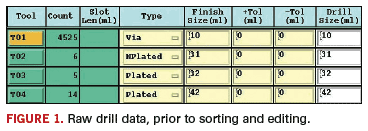
Step 2, Data manipulation. The first step is to ensure all artwork layers are aligned. Then drill data are compared to the hole chart on the fabrication drawing (Figure 1), and, if everything matches, the data are sorted into plated and unplated holes. (They are used at different times in the board fabrication process.)
Unplated drills are moved to a separate layer, and any copper target pads removed from their centers. Also, in our case the design was an array of multiple images, but the drill files were output as “one up,” so the drills had to be copied in a “step-and-repeat” pattern to match the artwork.
Any copper or silkscreen features that cross the board outline will be clipped to within 0.010˝ of the edge. Text or other drawn features outside the board edge will be removed.
If a netlist can be extracted from the CAD data, or if one is provided (preferably in IPC-D-356 format), it is compared to a netlist generated directly from the Gerber data, to look for discrepancies. If any mismatches are found, the job is placed “ON HOLD” and the customer is notified.
The following edits are made to improve the speed and accuracy of the design rule checks (DRC) performed in the next step:
Arcs created with a series of short segments are converted to a single smooth drawn arc.
Pads created with draws are converted to flashes.
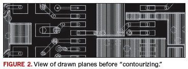
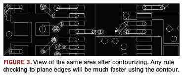
Planes created with draws are converted to a single polygon contour (Figures 2 and 3).
Legend detection identifies text on conductive layers, so the checking process won’t flag them as “hanging traces.”
SMD attributes detection identifies “pads without drills” to be understood as endpoints for netlist-checking later.
At this point, the netlist is re-verified to ensure any unintentional editing hasn’t altered the design integrity.
Step 3, Data verification. During this phase, several different rules are used to check the design, to ensure variations in fabrication processes will still produce a reliable circuit board. These rules are typically set by default in the CAM system, but are often customized to meet the unique requirements of the customer. Here’s what happened to my design:
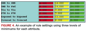
The minimum clearances and trace widths were identified. In our example, widths and clearances were collected and sorted into three categories: green, yellow and red. The green were OK, of course, but the yellow instances were approaching limits, and the red items highlighted the need for cost/yield considerations and maybe even the need to put the job on hold and consult with the customer (Figure 4).
The profile was checked. Measured were the copper feature distance to board edge, contours, cutouts and unplated holes (0.010˝ min.).
Drill diameters were compared to copper pad sizes to ensure sufficient annular ring for minimum acceptability.
Stubs and hangers were located and removed (or reported to the customer).
Step 4, Data preparation. Final modifications are then made to the data before they are sent to fabrication:
Solder resist layers are examined to see if apertures have been expanded or supplied as 1:1 match with copper. Modifications here may shrink or expand mask as necessary, and dam slivers may be removed, especially around fine-pitch SMT land patterns.
Silkscreen legend/nomenclature is clipped from exposed copper (solderable) surfaces, using the soldermask edges as a boundary/cutting edge.
Nonfunctional pads may be removed, depending on the default practices of the supplier or customer requirements.
Trace widths and/or dielectric spacing will be tuned to meet impedance requirements.
Compensation – copper feature dimensions may be increased to compensate for etching processes.
Pad teardropping may be added to reduce drill breakout in “conductor to land” junction area.
Company logo/UL marking and date code added to design.
Step 5, Data output. The data manipulation described in Step 4 was applied to the design as-received, while the following steps describe further manipulation to convert the design into production-ready tools. It would be difficult to list every possible variation, but every job will have a subset of these steps and have the same desired result (a working board that meets the customer’s requirements for the highest yield at the cheapest cost):
Individual or “palletized” designs (multiple boards placed in a single frame for ease of assembly) are arranged on the fabrication panel size (step and repeat).
Layers may be “stretched” to compensate for fabrication process tolerances downstream.
Tooling features, thieving and tracking/identification added.
Milling data are created to excise the final product from the fabrication panel.
Files for final electrical test are generated.
Layers in the “bottom half” of the stackup are mirrored.
The final task of Front-End Engineering is to output the final data into formats required by the specific fabrication equipment, and (if step-and-repeat was performed during CAM instead of CAD) send paste screen and palletization data to the customer.
Q&A
I asked several questions and discussed the answers with the FrontLine Users Group and several online discussion forums. This is a summary:
CAD: As designers, we are taught to define the data origin on a tooling hole if possible, but I never saw you use it for anything.
CAM: Maybe the origin is useful to someone down the line, but not to us. What’s more important is for all layers to have the same origin so they stack up correctly, including the drills.
CAD: I noticed you didn’t use the milling data we sent for routing the profile of the board. Why was that?
CAM: We don’t get that type of data very often. When we do, they usually are not optimized for manufacturing, and we have to modify them to minimize the tool path. It’s a simple matter to create, so don’t waste your time trying to provide it for us.
CAD: I noticed you changed the width of the features drawn on the silkscreen layers. Why was that?
CAM: From our experience, the customer doesn’t care about the width specifically; they just want it to be legible. Depending on the letter height, we adjust the width to work well in our process and give consistent results.
CAD: When you receive a note stating, “Data may not be modified without written approval,” do you perform the CAM job any differently?
CAM: Usually not. There are things we have to do to give you a good product, and the intention of the note does not pertain to those. Some customers are more than happy to have us fix things we find as part of the service we provide, but others would rather fix it themselves and send new data. Either way is fine with us, and learning each customer’s expectations is part of building a good relationship. Of course, we rely on written communications in all situations.
CAD: If you had one wish for improving the CAD-to-CAM process, what would it be?
CAM: (This is the only question that got multiple answers, which varied from “intelligent format” to “have every CAD operator spend a month in CAM, and every CAM operator spend a month on the shop floor” to “free ice-cream on Fridays.”)
Recommendations
Here are ideas for making this process more efficient and less susceptible to error. If possible, submit data in an intelligent format such as ODB++, but make sure the CAD system has implemented a reliable export capability. If you’re not sure, send a test file to prove your manufacturing partners can import it without difficulty.
(You may want to create Gerber data in parallel as a backup for suppliers who can’t import an intelligent format.)
If Gerber data must be sent:
Ensure the artwork layers and drilling files are created using the same format. (If you don’t know what to use, you probably can’t go wrong specifying ABSOLUTE, NO ZERO SUPRESSION and either 2:6 for coordinates in inches or 3:3 if the units are in metric.)
Create a separate layer for the board outline, or plot it only for the soldermask layers. You don’t want etched copper board outlines on every layer, or on the finished silkscreen.
Unless you are an expert, generate soldermask openings 1:1 with the pad sizes (except for fiducials). Unless the designer is known to have paid careful attention to expanding the soldermask apertures appropriately, the manufacturer would rather do it using a known starting place. Starting with mask that matches the pads makes the modification process much easier for the manufacturer.
If you are OK with removing nonfunctional pads, leave them in the design so they can be used for drill/annular ring checking, and the CAM operator can remove them later.
A unique aperture size used to draw planes, sized differently than any of the thermal spoke widths, can be very helpful to CAM.
Differentiate which holes are plated and which are unplated.
If leaving it to CAM to create an assembly array or pallet with breakaway tabs, make sure to leave spaces free of traces and components for the tabs.
ReadMe files are encouraged! Make sure to list any known netlist discrepancies.
Never try to perform your own etch compensation!
Finally, preview the final output before you send it out. You can find several free tools by searching the Web for “Gerber viewer.”
Jack Olson, CID+, is a circuit board designer at Caterpillar Inc. (caterpillar.com); This email address is being protected from spambots. You need JavaScript enabled to view it.. Mike Tucker is a technical service engineer at P.D. Circuits (pdcircuits.com).