
The right impedance ensures against additional SI or EMI issues.
A well-designed power distribution network (PDN) must have low impedance on the delivery path. The question is, How “low” is enough so that a PDN can deliver sufficient power supply for ICs to work properly? To answer this, we first need to define the impedance so that a PDN can be mathematically represented.
Suppose a PDN to be a linear network with named nodes and branches, and current flowing from VRM through PDN to ICs. The impedance at any location of a PDN can be defined as
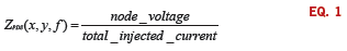
The impedance here is the ratio of actual node voltage change to the total dynamic current drawn by ICs at any frequency point. If the total current is normalized as 1, the node voltage at any location gives the impedance at that node. At a given frequency, when x and y are the coordinates of IC power supply pins, the impedance would be the one seen by an IC component to the PDN, which is what board or system designers are interested in, and needs to be minimized. Figure 1 illustrates a good PDN as it appears in the frequency domain.
It is important to emphasize the PDN impedance is defined in frequency domain. Then, how do we use it in a digital design, which works with transient signals in time domain?
Time domain considerations. Considering the power supply for an IC needs to be steady at a required DC level, and the IC can tolerate certain variation of DC voltage (ripple and sag), the DC voltage level and the tolerance give the variation range of power supply. Since the voltage changes in the time domain consist of frequency components at all frequencies, the goal of a PDN design can be described by the minimum range of voltage changes, and maximum current drawn by ICs. This is what we call the target impedance Zt

Here, the supply voltage and allowed ripples (in percentage) give the power supply budget, and the current is the worst transient current drawn by ICs connecting to PDN. Because voltage ripples and the worst transient current can happen at any frequency, this makes the target impedance independent of frequency. In practice, the target impedance, which is effective at all frequencies, is neither achievable nor necessary due to the limited switching speed of a physical IC.
Because the voltage ripples are caused by the combination of the switching currents of all ICs, which a PDN needs to provide power to, the term “current” in Eq. 2 represents actually the total allowable current to switch at the same time. It does not identify when and where individual switching currents occur. From this point, the target impedance in (2) is rather pessimistic; a design meeting the target impedance of (2) may not be an efficient one.
In high-speed digital designs, chips switch their states in sequence. Therefore, all switching current has its profile in time domain. When switching current with a certain profile happens, it means a time variation current source is applied to a PDN at one or several ports (IC power pins). This current induces voltage drops across PDN, which reveals the actual voltage a chip will get during its state changes.
The last question on IC current would be where a PDN designer can obtain switching current profiles. As discussed, the switching current represents the dynamic power consumption on chip, which consists of core and I/Os. Considering the simulation tools for board or package have no access to the IC database, and the chip structure is generally beyond the scale of board/package tools’ solving capacity, the best approach for getting accurate switching current profiles is to contact IC manufacturers that own power analysis tools and measurement equipment for chips. Fortunately, IC manufacturers are willing to provide such information to system designers.
One last caveat: This discussion about PDN impedance assumes a power delivery path ends at the BGA of a component mounting on a printed circuit board, and IC current is drawn directly at BGAs. In reality, the actual component on board includes chip and package, which introduce additional inductance and capacitance to be resonant with the rest of the PDN impedance. Package parasitics and on-die capacitance can be included in PDN if both models are available. However, the new PDN impedance becomes “component-dependent.” If a component is replaced by another, the impedance of the entire PDN needs to be reanalyzed. A better solution is to equip PI tools with user-preferred options about package and chip effects.

Although power integrity is relatively a new term in high-speed digital design and analysis, its concept has been used in designs for many years. The goal of power integrity is to have PDN provide sufficient power supply to ICs efficiently, without introducing additional SI or EMI problems. The important means to designing a good PDN is to make PDN impedance below predefined target impedance. PCD&F
Dr. Zhen Mu is product market manager at Mentor Graphics (mentor.com).


