Higher signaling speeds require better signal integrity, thus designing multi-GHz or multi-Gb boards has to involve better knowledge and tools than ever.
Ed.: Part 1 of this two-part series was published in November 2009.
Impedance measurements. Traditionally, impedance is measured by time domain reflectometry (TDR) on test coupons. Test coupons are manufactured on the same panels as the actual PCBs, and contain the same controlled-impedance traces (same width, same layer). Reason: It is easier to probe traces on a test coupon than on an actual, dense PCB.
TDR instruments generate a single very short pulse signal, and measure the reflected or arrived signal at the other end of the trace. Based on the TDR result voltage levels, the instrument or user performs some post-processing to get the measured impedance.
To take accurate frequency-dependent impedance measurements, set the TDR instrument to the same rise time as the signal would have on the actual PCB on the appropriate signal trace. (In practice, manufacturers don’t do this, although most TDR instruments have the option to set the rise time. Normally, a manufacturer has its favorite rise time setting and uses it for all measurements.) Some TDR instruments don’t have the option to set rise time; others do. This could lead to measuring impedance on a different frequency than it should be, and could result in a measurement error (Figure 8). The error is relative to the requirement, not an absolute value to the ideal impedance, since in reality, both the impedance requirement and the measurement are frequency-dependent.10
One way to do single frequency-point impedance measurement is to use a vector network analyzer (VNA) instead of a TDR. There are simple programs based on analytical equations, but they are outside of the scope of this article, as the calculation error can be 5 to 50%. Instead, we are focusing on field-solver programs, for which the only possible inaccuracies are the not-infinite mesh density, the wrong frequency, simplified modelling and improper usage. (For most programs, the software developers internally set mesh density.)
Field-solvers divide the geometry (2-D cross-section) into small pieces (nodes) – a process called meshing – and then solve the Maxwell’s differential equations in all of them to determine electrostatic and magnetic fields and current distribution (Figure 9).
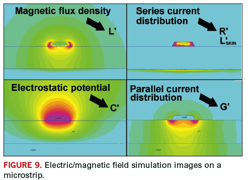
Next, as post-processing on these fields and currents, they determine the RLGC per-unit-length parameters. Finally, they calculate impedance as described. Typically, they calculate w –> Z0 directly, and if the opposite way of calculation is needed, then they iterate until they reach the desired characteristic impedance within a user-specified tolerance (0.1 to 5%). Some samples:
Polar Instruments Si8000. This is the industry standard frequency-independent impedance calculator. It calculates everything on 2 GHz. The Dk value must be pre-compensated to the signal’s frequency or to a suitable value. (For computer boards, 2 GHz is sufficient.) It calculates both width –> impedance and impedance –> width.
Polar Instruments Si9000. This is the extended version of the Si8000, with some frequency-dependent parameter calculations. It only calculates width –> impedance in a frequency-dependent form, and impedance –> width only in a frequency-independent way, or with manual iterations. For the former, it compensates (as an option) for Dk over frequency.
Polar Instruments Speedstack. A stackup builder, it uses Si8000 or Si9000 for impedance calculations, but its material library does not support frequency-dependent Dk specifications. So, in case of using together with Si9000, we need to override Dk, impedance and width values.
TNT-MMTL (open source; available at Sourceforge). Developed by the Mayo Clinic Special Purpose Processor Development Group, it can do both ways w –> Z0, and w –> Z0. In comparison with the Polar Si8000 in a few different tests, I calculated a maximum 2% difference for coated microstrips, and less than 1% for stripline structures. This is frequency-independent.11
Appcad RLGC. This program calculates the transmission line RLGC parameters, and the user has to calculate the impedance from them. This is frequency-dependent.12
General-purpose 2-D field-solvers. Examples include Ansoft Q3D Extractor, FEMM (FiniteElementMagnetics, open source). These programs provide the opportunity to set every simulation parameter, so they can be used on any levels of accuracy. We can draw any arbitrary-shaped cross-sections, and model multiple material platings on the conductors. They only work in the width (geometry) –> impedance way. They are normally frequency-dependent. The simulation setup may take several hours, since we have to hand-draw the geometry, do mesh seeding at critical areas and specify material parameters, perform simulations, and post-processing. After several simulations, we can get the RLGC parameters or matrices to use to calculate impedance.13
Frequency-Dependent Impedance Control Drawbacks
There are certain problems with frequency-dependent impedance control. For one, at the time of this writing, there was no available accurate, fast method/software to calculate trace width from impedance requirement on a user-specified frequency.
Second, PCB manufacturers do not perform frequency-dependent impedance measurements. They often say they do, but usually they have their choice of a specific signal rise time, yet it is fixed for all their measurements. The basic principles of TDR impedance measurements are frequency-independent. There is no method under which TDR could discern the test coupon impedance on a given frequency, since the TDR signal also is a wideband signal. One way could be to set the TDR test signal at a similar frequency spectrum as the digital signal, which – simplified – means setting the same rise time on the TDR as the digital signal. But it is not proven why it would be more accurate, and the theory remains under study.10
Third, there is no exact method found for time domain to frequency domain signal conversion. For digital signals, it is hard to select a single frequency, since they are wideband signals and defined in time domain. There could be several user-based choices (knee frequency, clock frequency, mean of band, etc.) to pick up as a part of the signal’s frequency spectrum. So, the selection leads to more inaccuracies.
Frequency-Independent Impedance Control
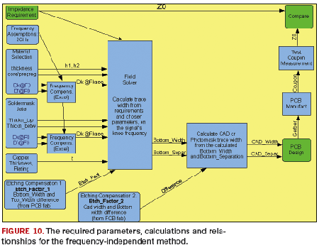
This is a subset of the previously described frequency-dependent method. On a certain level, it still must be frequency-dependent: As a minimum, we must compensate for the frequency dependence of the dielectric constant, since it usually is provided on a very low frequency (1 MHz). Before putting material Dk and Df information into the calculator or its library, compensate for them to a suitable frequency (e.g., for computer boards, 2 GHz is sufficient) (Figure 10).
The method is the same as described in the frequency-dependent calculation, with the following differences:
- The field-solver does not need the Df data, but the Dk compensation still does.
- The TDR measurements can be done with the usual constant rise time.
- Dk values can be set into a material library once, and don’t have to be overriden at every calculation, based on the signal’s frequency.
Available software provides a quick way for the impedance –> width calculation required for common product design.
We don’t care about the frequency spectrum of the digital signals in frequency-independent calculations.
Stackups and Signal Integrity
Crosstalk. There is no impedance control without crosstalk control. Maybe some do impedance control when not taking crosstalk into account, but the boards will behave unpredictably. If we change a stackup to achieve the impedance requirement, then the crosstalk levels also change.
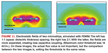
Crosstalk between traces on the same layer. Among several parameters, the trace separation versus dielectric thickness ratio (and not the width versus separation ratio) has a significant effect on crosstalk noise (Figure 11). If the dielectric material (thickness) is changed in the stackup, then the crosstalk levels between the traces change too. If thickness increases but trace-separation remains the same (between traces on the same layer), crosstalk increases. So, if it must be changed on a board post-prototype, only decrease the thicknesses (between signal layer and ground/reference plane); never increase them. Increasing the dielectric thickness will increase the ground return current areas and their overlapping (different signals) area. It also increases the mutual inductance and mutual capacitance. Crosstalk can be traced to mutual inductances and capacitances between traces, so they must remain low. A poor but widespread practice is to allow different fabricators to change the stackup based on their material stock. Material change usually means dielectric thickness change, which changes the crosstalk levels. Typically, those involved are too ill-informed to know they are changing the crosstalk levels too. To avoid problems, a design or signal integrity engineer must be involved in approving new stackups for existing boards, and they have to understand the effects. Otherwise, poor yields or field failures will occur at random.
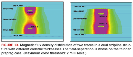
Crosstalk between traces on different layers (dual striplines). Since the two signal layers reside in each other’s magnetic and electrostatic fields (between the same two reference planes), there is a lot of parasitic inductance and capacitance between the traces. A usual technique is to perpendicularly (90°) route the signals on the two layers, avoiding long coupled segments between them. The crosstalk levels (mutual L, C) are higher for longer parallel trace segments. For complex digital boards, it usually is impossible to maintain 90° routing. Do not use dual striplines. (Use more ground planes.) Try to minimize the overlapping areas of the magnetic flux and electrostatic fields (Figure 13) on the two layers to minimize crosstalk. This can be accomplished by putting the signal layers closer to the two different reference planes, and farther from each other. Poor industry practice (changing stackups without approval by hardware or signal integrity engineers) has the same effect on this type of crosstalk as was described in the previous section: changing crosstalk levels without control or attention (indeterminate behavior).
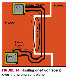
Crosstalk caused by return current discontinuities. When the return currents of multiple traces are forced away from their natural path to a plane-split edge, they induce noise currents into each other’s signals. Since the return current in these cases is not flowing underneath the traces but with a few millimeters offset, they create a current loop. One branch of the loop is the signal (signal current) and the other is the return current (Figure 14). For plane discontinuities, these loops of different signals overlap, and they effectively create a single-turn transformer between the signals, which creates strong crosstalk. The obvious response is to route all signals only above continous planes. Both planes must be continous for striplines, since the return currents flow in both planes (Figure 15).
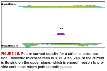
For stripline structures, provide the current return path in both planes, not only in the closer one, since the return current has its natural path in both planes. For dual striplines, both signal layers have return currents in both planes.
Layer change without stitching vias (or stitching/decoupling capacitors) also belongs to this problem group, since after pulling the signal through the stackup, we also have to provide the return current path through the stackup to the appropriate planes (between the reference planes of the start and the destination signal layers).
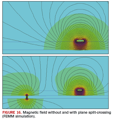
Impedance discontinuities. The trace impedance will be the same as the calculated value if there is a path provided in (both) the reference plane(s) where the return current can flow. If we cut its way (plane split), or the signal’s driver or receiver chip’s ground pin has no short (AC) connection to the reference plane(s), or there are voids on the plane (antipads), then the return current is forced away from its natuaral path (right underneath the signal trace with a specific current distribution shape), and the calculated impedance is no longer valid. It is a simplification to say the impedance is defined by the PCB cross-section geometry. In reality, it is defined by the shape of the distributed currents in both the trace and reference planes, and by the shape of the magnetic and electrostatic fields. These field shapes are guided by the geometry.
For example, a 100 µm wide microstrip trace over a 100 µm dielectric has an impedance on 1 GHz of 69.5Ω (based on FEMM RLGC simulation), but when the trace has to cross a plane split and go above the wrong plane in parallel to the split edge at a distance of 9 mm for awhile, then the impedance will be 158.9Ω, a huge difference (Figure 16). The reason is the modified current return path inside the reference planes, which increases ground path inductance. Another reason is that the trace capacitance (electrostatic field) now has to go through the plane split too, so the C parameter is decreased. If there is a big void on a reference plane, it creates the same problem: The return current cannot jump to the next plane for that part of the signal path, but only flows on continuous copper. In some cases (not between analog and noisy-digital grounds), this return current path can be provided by using stitching capacitors over the split.
The two main reasons why discontinuities are bad are 1) if 50Ω are needed and 150Ω are obtained, then obviously the impedance requirements are not met, and 2) discontinuities also significantly increase crosstalk and EMI.
3-D discontinuities. Via transitions, connectors and IC package pins create 3-D discontinuities that only can be modeled by 3-D electromagnetic simulators (e.g., Agilent Momentum, Ansoft HFSS, CST Microwave Studio, Cray-LC). These 3-D discontinuities create impedance deviation from the simply calculated values, and introduce parasitic inductances and capacitances into the signal path. The previously described discontinuities also are 3-D, but are so flat, they can be handled as 2-D discontinuities.
Conclusions
Not only must cross-section parameters be taken into account, but also other layers in the stackup, reference plane discontinuities, the used signals, the pattern on the copper layers, and so on. Because higher signaling speeds require better signal integrity, impedance control for today’s multi-GHz or multi-Gb boards has to involve more knowledge (PCB manufacturing technologies, high-frequency measurements, signal integrity, electromagnetism, material science) and more sophisticated tools than was necessary even a few years ago. One part of maintaining good signal integrity is to control impedances within a tight range.
For a quick way to perform everyday calculations for design, use a frequency-independent method for simplicity, with a few parameters considered on an average or usual constant signaling frequency. For computer motherboard designs, 2 GHz seems to give the best accuracy. The fully frequency-dependent method is not completely developed, especially not from the design point of view. It may be used for analysis for verifying the impedances. PCD&F
References
10. Simberian Inc., “Micro-strip Line Characteristic Impedance and TDR,” application note #2009_04, April 2009.
11. Mayo Clinic Special Purpose Processor Development Group, TNT MMTL freeware field solver program, http://mmtl.sourceforge.net/.
12. Applied Simulation Technology (Apsim), AppCAD RLGC, http://apsimtech.com/.
13. The field-simulations in this document were prepared in the Finite Element Method Magnetics (FEMM) freeware/opensource 2-D fieldsolver program (http://femm.
foster-miller.net).
Istvan Nagy is hardware design engineer at Concurrent Technologies (cct.co.uk); This email address is being protected from spambots. You need JavaScript enabled to view it..


