SI rules must take into account signal quality, timing and crosstalk.
Today’s high-speed busses, such as PCI-Express, DDR2/3, and serial ATA, running at frequencies from several hundred megahertz to beyond a gigahertz, make for tight timing margins. The fine-geometry silicon required for these speeds makes for very fast edge rates. And pressure for smaller and cheaper products makes for very dense PCB layouts. All these factors necessitate high-speed analysis, and the subsequent generation of routing constraints, to implement a successful high-speed printed circuit board design.
There are three main areas of concern when developing high-speed design constraints: signal quality, timing, and crosstalk. When taken together, these three factors can be called signal integrity (SI) constraints. Defining the constraints for each of these forms a set of SI rules, under which the design must be executed.
Signal quality includes items like overshoot, ringback and non-monotonicities: items that can damage a receiver or introduce data errors. Timing at the PCB level, including effects of terminations, receiver loading, and trace impedances and lengths, must be rigorously analyzed to ensure compliance at the system level. Crosstalk, which is unwanted noise induced by one trace onto another, can affect both signal quality and timing. Ensuring proper system operation requires all these analyses. The resulting constraints drive trace lengths, topology and spacing. This, in turn, drives items like parts placement. It is also necessary to constrain items like board stackup, trace widths, and copper weights. Clearly, high-speed PCB designs should not begin without the proper analysis.
Signal quality. Digital logic reduces data to a series of 1s and 0s, which are represented in a real system by high and low voltages. A receiver discerns whether a voltage represents a 1 or a 0 when that voltage is above or below the logic thresholds of the receiver. Also, that voltage must not exceed the limits (upper or lower) of the receiver, or it might be damaged. These two requirements generate two fundamental constraints in signal quality analysis: ringback and overshoot.
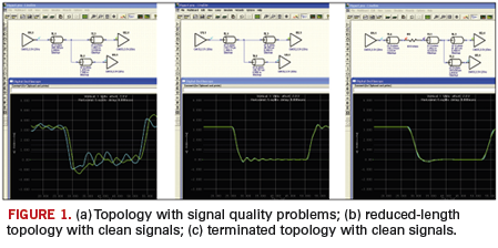
If a designer were to just connect a transmitter to two receivers, the result would be something like the waveform in Figure 1a. Here, ringback and overshoot violations can be seen. The green waveform, which is the receiver in the upper right of the topology, shows negative overshoot in excess of 1.4V (magnitude). The blue waveform, the other receiver, rings back to 0.8V, which is the lower logic threshold. If a PCB were built with this topology as is, errors in the data stream would occur, and the receivers could be damaged.
If the topology lengths are reduced significantly, to well below the length of the signal edges, these receiver waveforms get cleaned quite a bit (Figure 1b). Unfortunately, however, such lengths are typically on the order of an inch or so, which is not always feasible in a design.
Another method of cleaning the signal at the receiver is to use termination impedance. Termination matches the impedance of the drivers and receivers to the board traces, controlling the reflections that create overshoot and ringback violations. Using termination also permits much greater flexibility in the lengths of various parts of the topology. The trace lengths aren’t restricted to an unrealistic maximum, while still permitting clean signals.
Termination values may be taken from bus design guidelines, but in the absence of such guidelines, can be determined from analysis. Some tools determine the values for a termination automatically by looking at the topology. Beyond that, the location of the terminator within the trace topology can be determined by varying those lengths and analyzing the results. Maximum length rules for determining where the terminators may be placed are created from this analysis, as well as length constraints for the other traces in the topology (Figure 1c). All these lengths may be explored to create the widest solution space for the layout designer, which still meets the signal quality requirements.

Timing. Most length constraints in a design come about from a timing requirement. Timing requirements come from the fact that data are “clocked in” to a receiver at certain intervals. If the data are not there when the system needs them to be, it won’t work. There are two main types of bus timing architectures – common clock and source synchronous – that lead to two types of layout constraints: min./max. and matched lengths.
Minimum and maximum delay constraints are created from common-clock bus architectures. An example of this would be PCI, where data are clocked out of a transmitter and into a receiver using a common clock. To make sure the data are not there early, or violate the hold time requirement, a minimum length constraint must be created. To ensure the data do not arrive too late, a maximum length constraint is created. These constraints are not merely based on the length of the line, however. Many other considerations such as receiver loading and signal quality issues determine when the transmitted data may be valid at the receiver, so proper signal analysis must be performed to calculate these lengths appropriately.
Matched delay constraints come about from source-synchronous busses. These busses, such as DDR2, send a clocking signal or “strobe” along with the data to clock it in at the receiver. This eliminates the complex timing relationship between driver and receiver, and requires only the matching of the strobe to the data. Typically these interfaces have other concerns, such as signal quality, which determine when the data are valid. The main timing constraint for these busses is the matched delay constraint, which becomes tighter with increases in bus speed or signal quality problems.
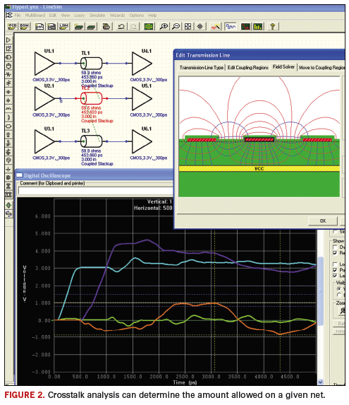
Crosstalk. Another important constraint for the layout is the spacing between traces. The spacing limit is determined by the amount of crosstalk that occurs between the signals. A number of factors influence crosstalk: the edge rate of the driver, the board layer stackup, the amount of parallelism between traces, and, of course, the spacing between traces. Crosstalk affects both signal quality and timing, and the amount of crosstalk allowed on a given net can be determined from simulation. An example of a crosstalk simulation is shown in Figure 2.

Crosstalk analysis typically consists of a “victim” trace and two “aggressor” traces. More aggressors can be included, but in most cases, 95% of the crosstalk will come from the nearest two. With models for the driver and receiver, as well as the board stackup built into the simulation, the spacing between the traces can be modified to determine an acceptable level of crosstalk. The length the traces run parallel also can be modified to view the effects. The main result of such an analysis is a spacing rule between traces. If that spacing rule could not be met, or if greater flexibility is to be permitted in the layout, a rule could be created with tighter spacing, but also with a maximum parallelism constraint. Such a pair of constraints could be created from crosstalk analysis, and modified as demands change.
Multi-gigabit/SERDES analysis. The same concerns of signal quality are at the forefront of analysis for SERDES busses such as PCI-Express and serial ATA. These busses do not have the same delay constraint as traditional, parallel busses, since they do not have an external clock. Most delay constraints associated with these kinds of busses are to match the two sides of the differential signal very closely. Because multi-gigabit signals use differential signaling, and have rise/fall times less than 100 ps, it is important to match both sides of the differential signal to less than 10 ps, which translates to a length of just tens of mils on a PCB. Crosstalk is also a concern on these busses, especially since they operate at lower voltages than 3.3V and 5V logic, and therefore are more susceptible to crosstalk from those signals. Crosstalk analysis is done on SERDES busses much as it is on other busses, and spacing from other signals will typically need to be much larger than is typical.
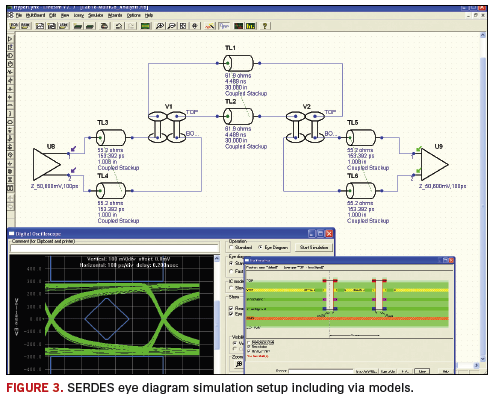
The biggest threat to multi-gigabit signals is loss. As frequencies increase, so do the loss effects. The biggest contributor to loss is length, which is why there are typically maximum length constraints on SERDES busses. Loss is also affected by the dielectric material used in the board, as well as the width of the traces carrying the signals. Other pieces of the signal path, such as vias, can also adversely affect the signals. All these effects are included in an appropriate eye diagram analysis, which gives a comprehensive view of the worst-case signals transmitted on the bus (Figure 3).

The results of such a SERDES analysis include maximum length constraints, trace width and spacing requirements, as well as layer constraints. Being able to explore changes in these items, such as modifying via geometries and layer changes, is vital to ensuring success in a SERDES design, while maximizing routability and flexibility in the layout.
Post-route verification. Once you have created all the necessary routing constraints for your design, and routed the board using those constraints, it is useful to verify that the board meets the original electrical requirements that prompted those constraints. Post-route signal analysis on all nets of a board is a good way to close this loop. Post-route analysis is an excellent complement to the rigorous pre-route or “what-if” analysis performed earlier in the design cycle. It is another step in the series of tasks performed to analyze high-speed busses.
Signal integrity analysis and verification is critical with high-speed designs. Signal integrity – signal quality, timing, and crosstalk – can result in data loss, errors, non-functioning circuitry, and even component damage if not controlled with a set of rules or constraints. Worse, many of these errors are highly intermittent, making them extremely difficult to fix after the fact, and component damage can be cumulative, meaning failures occur “down the road.” Without these types of analyses, and the constraints created as results, modern digital systems could not be designed to meet the cost, size, and performance needs of today. PCD&F
Patrick Carrier is a technical marketing engineer for high-speed PCB analysis tools at Mentor Graphics (mentor.com); This email address is being protected from spambots. You need JavaScript enabled to view it..


