What happens to CAD data once they are released to manufacturing?
How often does the fabrication drawing have a note that states something similar to this?
“DATA MAY NOT BE MODIFIED WITHOUT WRITTEN APPROVAL.”
Is it your intention that the board fabricator should make production tools from your data “AS IS” and run with it? If not, do you have a clear idea what modifications are acceptable?
Let’s imagine our responsibilities if we were working in the CAM department of a board manufacturer. Our customers are using different software tools for circuit board layout, using different rules and parameters, and creating output data in different formats. We can’t expect any two customers would do the same thing the same way. Our job would be to:
- Accept data from many sources.
- Analyze the data and customer requirements.
- Prove they are acceptable for our process.
- Modify the data, as needed.
- Output the data to consistent formats.
- Insert data as a smoothly running stream into manufacturing.
I recently had the opportunity to learn more about what happens to our data once we let go of it. I followed a typical job from our facility through manufacturing, and this is what happened.
Step 1, Data discovery. After the data passed through the Sales and Quoting department to Front-End Engineering, Frontline Genesis 2000 software was used to import it. (Other systems perform similar functions, and this process is not tied to any particular CAD or CAM software.)
Because designers have a variety of naming conventions for files, most CAM systems have a feature that automatically examines the file internally to interpret the data type and format settings. The software’s “best guess” is displayed on the screen. Once they are identified correctly, the artwork layers and drilling data are often renamed or labeled for consistency or to aid subsequent processes.
If there are any missing files, files that won’t load or obvious data errors, the job is put “ON HOLD” and the customer is notified.
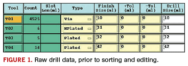
Step 2, Data manipulation. The first step is to ensure all artwork layers are aligned. Then drill data are compared to the hole chart on the fabrication drawing (Figure 1), and, if everything matches, the data are sorted into plated and unplated holes. (They are used at different times in the board fabrication process.)
Unplated drills are moved to a separate layer, and any copper target pads removed from their centers. Also, in our case the design was an array of multiple images, but the drill files were output as “one up,” so the drills had to be copied in a “step-and-repeat” pattern to match the artwork.
Any copper or silkscreen features that cross the board outline will be clipped to within 0.010˝ of the edge. Text or other drawn features outside the board edge will be removed.
If a netlist can be extracted from the CAD data, or if one is provided (preferably in IPC-D-356 format), it is compared to a netlist generated directly from the Gerber data, to look for discrepancies. If any mismatches are found, the job is placed “ON HOLD” and the customer is notified.
The following edits are made to improve the speed and accuracy of the design rule checks (DRC) performed in the next step:
- Arcs created with a series of short segments are converted to a single smooth drawn arc.
- Pads created with draws are converted to flashes.
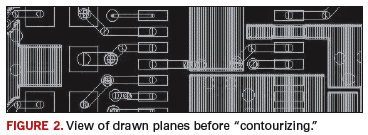
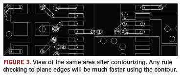
- Planes created with draws are converted to a single polygon contour (Figures 2 and 3).
- Legend detection identifies text on conductive layers, so the checking process won’t flag them as “hanging traces.”
- SMD attributes detection identifies “pads without drills” to be understood as endpoints for netlist-checking later.
At this point, the netlist is re-verified to ensure any unintentional editing hasn’t altered the design integrity.
Step 3, Data verification. During this phase, several different rules are used to check the design, to ensure variations in fabrication processes will still produce a reliable circuit board. These rules are typically set by default in the CAM system, but are often customized to meet the unique requirements of the customer. Here’s what happened to my design:
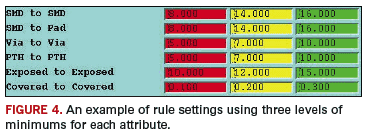
- The minimum clearances and trace widths were identified. In our example, widths and clearances were collected and sorted into three categories: green, yellow and red. The green were OK, of course, but the yellow instances were approaching limits, and the red items highlighted the need for cost/yield considerations and maybe even the need to put the job on hold and consult with the customer (Figure 4).
- The profile was checked. Measured were the copper feature distance to board edge, contours, cutouts and unplated holes (0.010˝ min.).
- Drill diameters were compared to copper pad sizes to ensure sufficient annular ring for minimum acceptability.
- Stubs and hangers were located and removed (or reported to the customer).
Step 4, Data preparation. Final modifications are then made to the data before they are sent to fabrication:
- Solder resist layers are examined to see if apertures have been expanded or supplied as 1:1 match with copper. Modifications here may shrink or expand mask as necessary, and dam slivers may be removed, especially around fine-pitch SMT land patterns.
- Silkscreen legend/nomenclature is clipped from exposed copper (solderable) surfaces, using the soldermask edges as a boundary/cutting edge.
- Nonfunctional pads may be removed, depending on the default practices of the supplier or customer requirements.
- Trace widths and/or dielectric spacing will be tuned to meet impedance requirements.
- Compensation – copper feature dimensions may be increased to compensate for etching processes.
- Pad teardropping may be added to reduce drill breakout in “conductor to land” junction area.
- Company logo/UL marking and date code added to design.
Step 5, Data output. The data manipulation described in Step 4 was applied to the design as-received, while the following steps describe further manipulation to convert the design into production-ready tools. It would be difficult to list every possible variation, but every job will have a subset of these steps and have the same desired result (a working board that meets the customer’s requirements for the highest yield at the cheapest cost):
- Individual or “palletized” designs (multiple boards placed in a single frame for ease of assembly) are arranged on the fabrication panel size (step and repeat).
- Layers may be “stretched” to compensate for fabrication process tolerances downstream.
- Tooling features, thieving and tracking/identification added.
- Milling data are created to excise the final product from the fabrication panel.
- Files for final electrical test are generated.
- Layers in the “bottom half” of the stackup are mirrored.
The final task of Front-End Engineering is to output the final data into formats required by the specific fabrication equipment, and (if step-and-repeat was performed during CAM instead of CAD) send paste screen and palletization data to the customer.
Q&A
I asked several questions and discussed the answers with the FrontLine Users Group and several online discussion forums. This is a summary:
CAD: As designers, we are taught to define the data origin on a tooling hole if possible, but I never saw you use it for anything.
CAM: Maybe the origin is useful to someone down the line, but not to us. What’s more important is for all layers to have the same origin so they stack up correctly, including the drills.
CAD: I noticed you didn’t use the milling data we sent for routing the profile of the board. Why was that?
CAM: We don’t get that type of data very often. When we do, they usually are not optimized for manufacturing, and we have to modify them to minimize the tool path. It’s a simple matter to create, so don’t waste your time trying to provide it for us.
CAD: I noticed you changed the width of the features drawn on the silkscreen layers. Why was that?
CAM: From our experience, the customer doesn’t care about the width specifically; they just want it to be legible. Depending on the letter height, we adjust the width to work well in our process and give consistent results.
CAD: When you receive a note stating, “Data may not be modified without written approval,” do you perform the CAM job any differently?
CAM: Usually not. There are things we have to do to give you a good product, and the intention of the note does not pertain to those. Some customers are more than happy to have us fix things we find as part of the service we provide, but others would rather fix it themselves and send new data. Either way is fine with us, and learning each customer’s expectations is part of building a good relationship. Of course, we rely on written communications in all situations.
CAD: If you had one wish for improving the CAD-to-CAM process, what would it be?
CAM: (This is the only question that got multiple answers, which varied from “intelligent format” to “have every CAD operator spend a month in CAM, and every CAM operator spend a month on the shop floor” to “free ice-cream on Fridays.”)
Recommendations
Here are ideas for making this process more efficient and less susceptible to error. If possible, submit data in an intelligent format such as ODB++, but make sure the CAD system has implemented a reliable export capability. If you’re not sure, send a test file to prove your manufacturing partners can import it without difficulty.
(You may want to create Gerber data in parallel as a backup for suppliers who can’t import an intelligent format.)
If Gerber data must be sent:
- Ensure the artwork layers and drilling files are created using the same format. (If you don’t know what to use, you probably can’t go wrong specifying ABSOLUTE, NO ZERO SUPRESSION and either 2:6 for coordinates in inches or 3:3 if the units are in metric.)
- Create a separate layer for the board outline, or plot it only for the soldermask layers. You don’t want etched copper board outlines on every layer, or on the finished silkscreen.
- Unless you are an expert, generate soldermask openings 1:1 with the pad sizes (except for fiducials). Unless the designer is known to have paid careful attention to expanding the soldermask apertures appropriately, the manufacturer would rather do it using a known starting place. Starting with mask that matches the pads makes the modification process much easier for the manufacturer.
- If you are OK with removing nonfunctional pads, leave them in the design so they can be used for drill/annular ring checking, and the CAM operator can remove them later.
- A unique aperture size used to draw planes, sized differently than any of the thermal spoke widths, can be very helpful to CAM.
- Differentiate which holes are plated and which are unplated.
- If leaving it to CAM to create an assembly array or pallet with breakaway tabs, make sure to leave spaces free of traces and components for the tabs.
- ReadMe files are encouraged! Make sure to list any known netlist discrepancies.
- Never try to perform your own etch compensation!
Finally, preview the final output before you send it out. You can find several free tools by searching the Web for “Gerber viewer.”
Jack Olson, CID+, is a circuit board designer at Caterpillar Inc. (caterpillar.com); This email address is being protected from spambots. You need JavaScript enabled to view it.. Mike Tucker is a technical service engineer at P.D. Circuits (pdcircuits.com).


