Positioning CSPs and noise-sensitive devices are two of a host of considerations.
Effective, accurate component placement takes into account the best practices of design and assembly, both of them inextricably intertwined. The layout engineer must take special care to correctly place components on the board, since this has a direct bearing on assembly and testability.
Also, with the evolution of various technologies, assembly takes on newer meanings, dimensions, and demands. In particular, use of fine-pitch BGAs is escalating, challenging current assembly practices and procedures. In these situations, PCB design and assembly know-how and experience are the linchpins for effective placement.
Design for assembly takes into account such factors as through-hole versus surface mount components, critical ribbon and cable assemblies, cutouts, vias, decoupling capacitor placement, mechanical aspects, and others. Through-hole technology has become more of a specialty, while surface mount is the basis for most of today’s designs.
In terms of placement and routing, the beauty of an SMT design is its superior leverage relative to board’s real estate area, because both sides of a board can be utilized. This creates certain challenges, however. For instance, an experienced PCB designer doesn’t want to place a noise-generating device or high–frequency, sensitive device close to the clock where the signal will incur interference. Improper component placement raises the probability of high-level noise and an unacceptable signal-to-noise (SNR) ratio.
Through-hole mostly is used for connectors and mostly is limited to signals coming into and exiting the PCB. However, SMT connectors increasingly are used. But some applications employ a combination of surface mount and PTH components. When a PTH connector is used, another component cannot be placed on the other side of the board since there’s no usable real estate.
The advantage of a surface mount connector is both sides can be used for component placement. However, the PCB designer must take precautions when placing either PTH or SMT I/O components. The same concepts apply to other components with gold fingers, ribbons, or cables attached to the board. Usually, the physical location of these devices is fixed. For example, a gold finger of a daughtercard going into a motherboard needs to be at a certain location to ensure a proper fit. At the same time, the board designer must ensure space limitations are not violated and no mechanical, vibration, or height-related issues are created due to that particular placement.
The designer also must check that all X and Y coordinate calculations are accurate. This means the cutout or gold finger is made at the right location because if a hole is off by, say, 0.010˝ to 0.020˝, then a pre-selected cable will not go in the right place. Physical location and dimension calculations cannot be fudged if I/O components are to precisely communicate with fixed devices from other systems or subsystems to the PCB.
As for vias, there are an array of types, including blind, buried, stacked, and through-hole vias. A through-hole via goes from one side of the board to the other. Blind vias go from an outerlayer to a middle layer; for example, a blind via originates at the top layer and terminates at one of the innerlayers. Buried vias originate and terminate within innerlayers. Stacked vias originate from each of the outerlayers and terminate on the innerlayers at the identical location.
When it comes to selecting vias for accurate component placement, the designer must consider the pros and cons of each to avoid assembly issues later. For example, for smaller and handheld devices, which are compact in terms of available real estate, there is sometimes no choice but to use blind or buried vias. These particular vias are difficult to fabricate and increase manufacturing cost. The advantage of these vias is that routing and connections use the innerlayers, thereby saving top and bottom layers for component placement and critical routing.
Signal integrity is another major DfA aspect when it comes to component placement. It is critical to appropriately place bypass capacitors next to BGAs, CSPs or QFNs. This is especially true in high-speed designs, for which transmit and receive paths must be highly accurate and extremely short, to avoid impedance control issues. The signal from a BGA ball to a bypass capacitor must be cleanly filtered to suppress noises, hence the importance of maintaining close proximity and placement of these capacitors next to BGA, CSPs and QFNs.
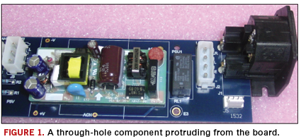
If the board has too many components close to the edge and protruding from the board (Figure 1), it’s best to use tab and route, versus scoring during board fabrication. By using tab and route, there is a small portion of rail to separate two boards from each other. On the other hand, a scoring device separates boards next to each other and is not ideally suited for boards with protruding devices.
Also, for efficient assembly involving small board sizes that are panelized, create accurate fixtures for handling PCBs during reflow soldering. But a panel must not be made too large; optimal panel size must be calculated to maximize manufacturing efficiencies. Otherwise, the board could warp from the component weight.
Aside from proper assembly techniques, DfA compliance also deals with different tools and the point to deploy them during assembly. For instance, will x-ray be applied as a process check at the end of each board or for sampling one of every five, 10, or 20 boards? When will a certain fixture be used? During surface mount? Wave solder? Or maybe at AOI or testing? These issues need to be addressed at the planning stage, when the CAM engineering/planning department is reviewing the data and preparing the processes and visual aids for the jobs.
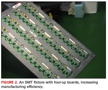
Not all machines will be able to use the same fixture, due to varying dimensions. But they will be different because they’re created to conform to different board sizes. Moreover, they have their own mechanical and tolerance limitations. Be aware of these tolerances, as a universal fixture is not a cure-all. At times, there must be multiple fixtures, one for SMT (Figure 2), another for wave solder, and still another for testing. Most often this occurs when boards are smaller and not uniform. For example, they may be semi-circular, round, half moon or L-shaped. In these cases, various types of fixtures are used to make assembly an easy, reliable and repeatable process.
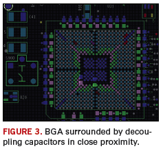
As far as BGAs are concerned, they demand special scrutiny and attention. BGAs require just the right amount of solder paste. Too much could cause shorts between the balls. Then there’s no choice except to depopulate and re-ball it, or use a new BGA device. Moreover, it’s important to ensure correct placement, keeping in mind component orientations and polarities. When rework is involved, sometimes it is important to desolder the nearby decoupling capacitors (Figure 3) or other devices, making rework possible.
Also, BGAs should never be placed close to the board’s edge. Reason: A BGA needs a peripheral area that’s heated during rework. If close to the edge, then that half side close to the edge will not sufficiently heat, simply because there’s no mass around the BGA device to heat. Hence, the BGA will be extremely difficult to depopulate.
At the stencil design stage, sound assembly practices depend on the decisions over foil thickness, stencil frames, aperture to pad ratio, for dispensing correct amounts of solder paste, when to use window panes, performing first article inspection, and the right type of solder paste, along with use of paste height measurement systems.
Foil thickness determines the amount of paste to be dispensed. Assembly personnel must determine whether a stencil will be 0.04˝, 0.06˝ or 0.08˝ thick to gauge the amount of paste required. As foil thickness changes, it changes the amount of paste dispensed on pads, thereby affecting the thermal profile.
Foil should come framed from a vendor. Stencil foils without frames create time and reliability issues. Time-consuming mistakes may include mounting the foil upside down or in reverse, and damaging it. Also, when stencil foils are not stretched properly when mounted on the adapter, it can adversely affect the quality of the paste deposit, causing bridging and misregistration on the SMT pads.
Aperture-to-pad ratio decisions, for example, can be whether those ratios will be 1:1, 1.1:1 or 0.9:1. The ratio 1:1 means size of the stencil opening is equal to the SMT pad. A 0.9:1 ratio means the size of the stencil opening is smaller than the SMT pad, thereby dispensing smaller amounts of paste. This mostly is used in ultra-fine-pitch SMT applications.
Sometimes a stencil opening is made a bit larger compared to the pad size so that the aperture to pad ratio becomes 1.1:1. This permits slightly more paste to be dispensed on the stencil. This is mostly used in heavy analog applications. In each case, assembly personnel must be fully aware of a board’s end application and whether the dispensed solder paste is adequate. Some studies have found as much as 75% of defects are related to paste dispensing, which bears directly on stencil design.
Window panes are implemented when there is a huge opening on a stencil design. Consider a 0.5˝ x 0.25˝ opening, which is extremely large when it comes to dispensing paste. Therefore, a decision is made to pane the window to create smaller window or opening sizes within the large opening. For example, six different slots or panes may be created to control the amount of paste going to these different panes versus applying a whole blob of paste on the pad.
Also, every time a decision is made involving stencil design, it’s vital to perform a first-article check to ensure the proper amount of paste is dispensed, or whether another foil needs to be cut due to a thickness or aperture-to-pad ratio change. This would act as a process verification tool for dispensing the right amount of paste on the pads.
Here’s where a first-article inspection system proves invaluable. FAI systems are relatively new. They help create the first-article board by scanning the image of the whole board (the golden board), and comparing the images of all other boards with this golden board to ensure all components are placed properly, with correct orientation and polarities. It is used as a process verification and inspection tool to significantly reduce the human interface and make inspection and QC more reliable, repeatable, and faster by at least 30 to 50%.
Last, solder paste and its varieties are vital considerations for accurate component placement. Normally, Type 2 and 3 solder pastes are used for analog devices and analog/digital. Sometimes Type 4 (or finer) is required for fine-pitch BGAs, CSPs, and QFNs.
Generally speaking, solder paste is a mix of metal grains and certain chemicals in a format conducive for soldering. Those metals are of considerably finer grain in Type 4 compared to Type 3. This means Type 4 can be used more accurately for fine-pitch components because its tolerance is slightly higher compared to Types 2 and 3. Viscosity for Type 4 is finer. This means grain particles are joined tighter together compared to those of Type 3, and thus can be used more accurately for fine-pitch components.
Zulki Khan is president and founder of Nexlogic Technologies (nexlogic.com); This email address is being protected from spambots. You need JavaScript enabled to view it..


