Written by Hiroshi Hoshiyama, Shinjiroh Hayashi, Makoto Sakai and Rikiya Shimizu
Category: 2010 Issues
A novel process is said to improve product interconnection and mechanical reliability.
Today, the most common flexible printed circuit substrates are 12.5 - 25 µm thick, with the trend toward even thinner materials. Two primary types of copper foil are used for flex: electrolytic copper foil and rolled copper foil. Electrolytic copper foils typically come in thicknesses of 18 or 12 µm, while most rolled copper foils are 18 µm thick. As with polyimide substrates, both types of copper foils are moving to thinner dimensions. Generally, rolled copper foils demonstrate flexural properties superior to those of electrolytic copper foil. Applications that require very high degrees of flexibility and reliability, such as HDD read-write heads, are dominated by rolled copper foils. However, in recent years, the flexural properties of electrolytic copper foil have been greatly improved and are gaining share in optical pickup applications.
Each of the three FPC categories – single-sided, double-sided, multilayer – requires somewhat different manufacturing processes. In addition, manufacturing processes for multilayer FPCs vary significantly, depending on the specifics of the desired circuit structure and performance characteristics.
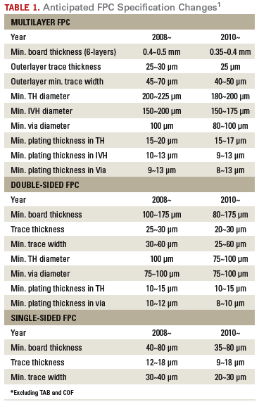
Table 1 demonstrates the evolution of FPC specifications. Design rules are changing to support miniaturization and multi-functionality. Trace widths and board thicknesses are becoming smaller. Minimum plating thicknesses are falling, leading to higher demands on the performance of plated copper deposits.
During double-sided/multilayer FPC manufacturing, metallization is employed to provide robust electric connections between layers. These processes represent critical steps within the overall production sequence. Typically, a combination of electroless copper plating and electrolytic copper plating is used to form plated through-holes and vias. Direct plate processes also are now widely used for initial metallization prior to electrolytic copper plating, especially for double-sided FPC.
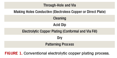
Electrolytic copper plating has a significant impact on FPC manufacture, as it affects wiring design, board dimensional tolerances and thermal/mechanical reliability. Figure 1 illustrates a conventional process flow for electrolytic copper plating. Electrolytic copper plating is carried out after the process steps of through-hole/via-hole formation, initial metallization process and pre-cleaning. Plated panels are dried prior to the patterning process. Since FPCs are thin and flexible, these features must be considered in their design and handling.
Electroplated copper deposits must have the following characteristics:
Dimensional stability after plating (ensures stable wiring dimensions).
Thermal/mechanical reliability (delivers appropriate performance for end-use environment and device assembly).
Compatible with full range of making holes conductive chemistries.
Uniform plating distribution on board surface (allows consistent circuit feature formation).
Plating surface smoothness (eliminates surface defects that might reduce manufacturing yield or degrade flexural performance).
Trends toward finer feature dimensions and higher interconnection densities require improved functionality from FPC electrolytic copper plating processes.
The attributes and benefits of a new electrolytic copper plating process are illustrated by comparison with the performance of conventional processes.
Dimensional stability. In response to finer feature and higher interconnection density trends, registration tolerance has to be improved. Improved substrate dimensional stability during manufacturing is required to meet these targets for registration tolerance. The main factors affecting dimensional stability during FPC manufacturing are base material performance, plating deposit properties and manufacturing process conditions. Internal stress within electrolytic copper plating deposits plays an important part in determining the overall dimensional stability. The effect of plating stress manifests itself as either bowing of boards after etching or patterning, or as shifts in pattern feature locations. The board dimensions shrink when the deposit has tensile deposit stress and expands under compressive stress. FPCs are particularly influenced by internal stress because the boards are so thin and flexible.
Typically, the internal stress of acid copper deposits is tensile. The amount of internal stress changes gradually, due to structural changes associated with self-annealing of the deposit. A copper plating process having low internal stress is therefore preferred for FPC applications.
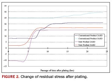
A spiral contractometer is most commonly used to measure stress in plated coatings. The deposit is formed on the exterior surface of a spiral shaped metal substrate, which is tightly secured at the lower end but free to move at the upper end. The interior surface is coated with an organic material to prevent deposition. Stresses within the deposit lead to either an opening or a tightening of the spriral, measured as an angular deflection of an indicator connected to the upper end. The deflection, combined with information on deposit thickness, then can be converted into a value for stress.
Figure 2 shows the residual stress for a conventional plating system and a newly developed bath, as a function of time after plating and plating current density. In a conventional process, deposit internal stress stabilizes between 20 - 30 MPa after 10 hr. While this level of residual stress is unlikely to have significant impacts on present FPC designs, it presents an issue for future design specifications. The new process shows an internal stress that reaches a value of approximately 15 MPa after 7 hr., and then remains stable. The residual stress is significantly lower than conventional processes.
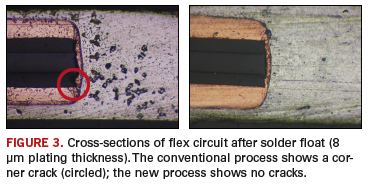
Thermal/mechanical reliability. Pb-free processing means higher assembly temperatures, placing greater demands on thermal reliability. The physical properties of electrolytic copper plating deposits must be enhanced to respond to these changes in assembly conditions and the trend toward finer feature dimensions. Figure 3 shows cross-sections of through-holes in FPCs after solder float testing and describes the substrate construction and test procedure. In general, when the plated deposits are thin (as is often the case in FPC applications), interconnection failures such as cracks tend to occur as a result of thermal shock. In tests, the new product shows excellent performance, even when used at low plating thicknesses. This provides an improved process window during assembly operations.
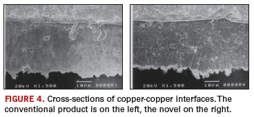
Compatibility with alternative metallization processes. Direct plating processes are widely used for the initial metallization of general-purpose, double-sided FPC. Compared to electroless copper plating, the resistance of the initial direct plate film is high, which poses a risk of deposition failure in the subsequent electrolytic copper plating process. In such cases, powdery copper deposits may be formed during the early stages of plating, resulting in adhesion defects and poor appearance. The new process has been found to show excellent compatibility with both a wide range of electroless copper and direct plate processes, providing excellent copper-to-copper interface quality (Figure 4).
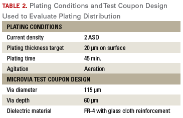
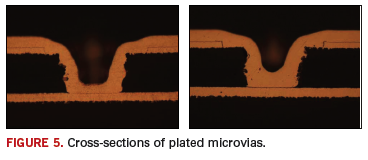
Plating distribution. Thinner copper foils and plated copper deposits and microvias are essential for increasing circuit density. High-density multilayer FPCs employ microvias for innerlayer connections. Consistent and uniform plating distribution is required to ensure optimum connection reliability, particularly for smaller diameter microvias (Table 2). Figure 5 compares coverage capabilities of electrolytic copper plating on microvias. The new process shows improved capability, even for small diameter vias, due to its plating coverage and distribution.
Surface smoothness. In contrast to rigid boards, FPCs require very high degrees of deposit flexibility. Bend test requirements for the FPC section that acts as an interconnection between boards vary widely with application. In the case of the interconnection within the hinge of a cell phone, more than 100,000 flexures are required (measured using a 180° open/close test).2
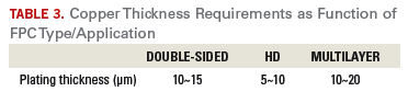
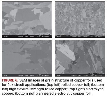
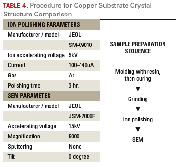
The area undergoing the bending operation must have a thin copper deposit in order to meet these needs. Table 3 shows examples of typical electrolytic copper plating thicknesses as a function of FPC type. FPCs used for moving parts generally use rolled copper foils, due to their superior bending performance. However, when electrolytic copper plating is applied over rolled copper foil, some degree of surface unevenness can sometimes be observed on the plated deposit. This is believed caused by an interaction between the plating process and the crystal structure of the foil substrate (Figure 6).
Ion polishing was used to prepare samples, which illustrate the differences in crystal structures between four different copper substrate materials (Table 4).
Unannealed electrolytic foils have relatively smaller grain sizes, while the grain sizes of rolled or annealed electroplated foils are larger (Figure 6).
Surface unevenness may lead to defects in subsequent imaging processes and can therefore become a major obstacle to high yield manufacture of finer line high-density FPC. To reduce the unevenness, higher plating thicknesses or mechanical polishing have been considered. However, thicker films have been observed to degrade flexural performance, and mechanical polishing is very difficult to perform, due to flex’s thin and soft properties. Electrolytic copper plating processes are required to produce deposits with excellent surface smoothness on all copper foils used for FPC to permit finer patterning and higher bending performance at reduced deposition thicknesses and without mechanical polishing.
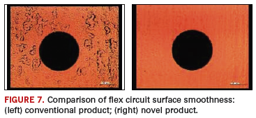
When plating on rolled copper foils, conventional products often show some fine surface unevenness and a semi-bright appearance. In contrast, no surface unevenness is found with the novel product and good brightness is observed. The new process permits reduced plating thicknesses with excellent plated surface smoothness, which provides both fine patterning capability and improved flexural performance.
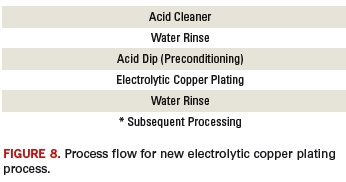
Figure 7 shows a comparison of deposit brightness between a conventional process and the new process. The latter does not require special process control, and conventional plating equipment may be used. Figure 8 shows the process flow of the new electrolytic copper plating.
Ed.: Portions of this article were previously published.
References
1. Japan Jisso Technology Roadmap 2007, pp. 55-57, 63-65, 69-70. 2. M. Watanabe, H. Sakurai, and T. Kanagawa, ”The Future Trend and Characteristics of FPC,” Fujikura Gihou, vol. 109, pg. 33-34, 2005.
Hiroshi Hoshiyama is interconnect technology R&D director Japan; Shinjiroh Hayashi is interconnect technology R&D project leader; Makoto Sakai is interconnect technology R&D scientist, and Rikiya Shimizu is interconnect technology Japan/Korea marketing manager at Rohm and Haas Electronic Materials KK, a Dow Group Co. (rohmhaas.com).
That wonderful RF spectrum may offer functionality and job security.
Recently I was talking to my friend Charley Capers of Trilogy Circuits in Dallas. Charley and I talk regularly on what’s going on in the PCB world and, of course, to stay current on our beloved Dallas Cowboys. (I am writing this the week after they won their first playoff game. If things don’t go well, you may hear some cursing by the time this comes out.) Charley mentioned that Trilogy has carved out a nice niche in RF design. This struck a chord with me because I remember doing some RF and microwave designs back in the 1980s. Then, we talked in terms of 1 GHz. Charley, however, was talking about frequencies in the multiple gigahertz range. This piqued my interest, so I started calling around.
It turns out that while RF may not be considered mainstream right now, it does account for a lot of designs. RFID is one technology that comes to mind, but with the exception of some silicon-based RFIDs, it is considered by most to be a low-tech design. But if you consider all the commercial products that use wireless communications, you’re still talking about a lot of circuit boards. Looking at the top of my desk, there’s a cellphone, the wireless connection to my server, a wireless printer, a Bluetooth headset for the cellphone, and a wireless keyboard and mouse. If I were to inventory my house and office, I’m sure I would find quite a few more wireless applications.
Of course, those applications are all in the 2.5 GHz range or less. Charley was talking about designs in the 10 GHz range and higher. According to my old frequency spectrum chart, “superhigh” or microwave frequencies start around 3 GHz, and “extremely high” frequencies (EHF) start around 30 GHz and go up to around 300. The designs Charley refers to are military applications such as radar, missiles and guidance control systems. But others such as airport x-ray scanners are becoming part of our everyday world and will incorporate frequencies in the RF and microwave spectra.
I also spoke with Dale Hanzelka, a principle applications engineer with Atlanta’s Intercept Technologies. Intercept is an EDA company that specializes in RF and other high-speed designs. Dale agreed there is still some black magic to RF design. A good portion of the layout is shape-based, and many of the physical features have to be “tuned” to that particular design. These parameters are difficult, if not impossible, to define at the schematic level. As a result, many engineers use products like AutoCAD to do the layout. While AutoCAD may get the physical features right, and could still generate Gerber files, there is no intelligence to the data. Some companies even have gone to the extent of developing in-house applications to work with AutoCAD instead of finding a CAD application specifically designed for RF and microwave designs. I asked if that means we’re talking about trial-and-error and iterations of prototypes to get things right. That was the old-school approach, Dale told me. Today, the best process is to do the layout and use modern tools to analyze and simulate the design before going to fabrication.
Dale also talked about applications like hybrid designs that include cavities in the substrate and wirebonding, which start to separate the everyday designers from RF and microwave specialists. As more wireless products become integrated in our lives, being one of those designers who knows as much as possible about RF may be a form of job security. Throughout the coming months, we’ll try to do our part by including some more features and columns on RF and microwave design in the magazine and address them at our conferences.
And just to show how deep into our lives this can go, Dale mentioned that for Christmas his wife received a handheld bar scanner. This handy little gadget sounds interesting. For instance, before throwing away that empty milk carton, she can run the scanner over the barcode and add the information to her shopping list. I suppose the next step would be to beam the grocery list to a Blackberry or other handheld device. That’s the kind of gadget that Uncle Pete could go for.
On another note, I want to remind everyone that Virtual PCB, the only virtual trade show and conference for the PCB industry, takes place March 2-4 at your place. Yes, you can attend the conference and trade show without ever leaving the comfort of your home or office. Registration is free, so go to www.virtual-pcb.com for more information.
Pete Waddell is the design technical editor of PCD&F (pcdandf.com); This email address is being protected from spambots. You need JavaScript enabled to view it..
A host of new specifications aims to overcome coverage issues brought on by high-speed circuits.
The influx of high-speed signals on boards, and the challenge to the test environment, has invigorated interest in limited access methodologies such as boundary scan and built-in self-test (BIST). The industry is gearing toward adopting key initiatives to IEEE standards, so as to be able to help resolve these test challenges. The following are the proposals to extend IEEE Standard 1149.1 boundary scan capability into embedded testing, as well as the BIST currently in use by OEMs in the semiconductor and board design areas.
IEEE P1687
The challenge. Board assemblies increasingly are populated with high-speed semiconductors and memory in the GHz range. As a result, placing testpoints on the PCB traces is nearly impossible, as it would degrade signal integrity. Without these testpoints, manufacturers will no longer be able to use ICT to capture defects such as opens, shorts and wrong component values. In turn, this would increase test and overall manufacturing costs.
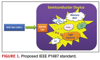
The proposed solution. OEMs and EMS providers are well aware of these challenges. Their need for a viable solution paved the way for the surge in interest in the IEEE P1687 standard, also known as Instrument JTAG or iJTAG. The objective of iJTAG is to develop a method and rules to access the instrumentation embedded into a semiconductor device without the need to define the instruments or their features using IEEE Standard 1149.1. The proposed standard would include a description language that specifies an interface to help communicate with the internal embedded instrumentation and features within the semiconductor device (Figure 1).
The purpose of the P1687 or iJTAG initiative is to provide an extension to IEEE 1149.1 specifically aimed at using the TAP to manage the configuration, operation and collection of data from this embedded instrumentation circuitry.
The benefit. With the proposed IEEE P1687 standard, test equipment providers will be able to access the embedded instruments in the semiconductor devices for testing purposes. At the same time, electronics manufacturers will be able to regain test coverage with minimal cost impact by integrating this solution into their current test process. Here are some ways in which P1687 can be implemented on the manufacturing floor:
1. Integrated into existing ICT. 2. ICT system > P1687 test solution. 3. P1687 test solution > functional test. 4. Integrated into existing functional test.
Among the possible implementations for P1687, integration into the ICT system would most benefit manufacturers, as the majority of high-volume companies use ICT to screen structural defects. With this implementation, EMS companies would be able to increase the value of their ICT and avoid a costly investment in another system to cover both the analog and digital defects of the assembly.
IEEE P1581
The challenge. One of the most common devices today is Dynamic Data Rate (DDR) memory, which can be found on everything from netbook motherboards to a larger high-end server and telecommunications boards. The challenge in testing memory devices lies in the high clock speeds for DDR memory, which now run in the GHz range. Again, with such clock speeds, testpoints would no longer be viable. The lost coverage means failures could only be captured after ICT, where finding defects and repairing them would be five times more costly.
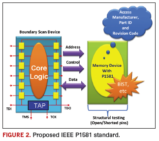
The proposed solution. The proposed IEEE P1581 (Figure 2) aims to develop a standard method for testing low-cost, complex DDR memory devices, which would be able to communicate through another semiconductor device with an IEEE 1149.1 boundary scan capability. Presently, even if DDR memory devices adopt the IEEE 1149.1 boundary scan standard, this is still not a feasible test, as it will require the addition of the four mandatory TAP pins to the DDR device, which would add to the devices’ complexity and cost. P1581 would provide the protocol to access the test mode within the memory devices, without the need for dedicated test pin requirements. The defined standard for this new test technology would enable each vendor to create its own method for implementing test hardware functionality in memory devices. It guides them on the necessary implementation rules for access and exit test modes. In contrast to IEEE 1149.1, this standard provides a static test method and requires fewer test pins. The standard would also allow implementation of P1581 on other semiconductor devices besides memory devices.
The benefit. P1581 would help the DDR memory vendor to enable its memory devices to communicate with boundary scan-enabled devices. Manufacturers would regain the test coverage on DDR memory that even current standalone solutions like 1149.1 are finding hard to run with any good measure of stability due to high clock speeds.
IEEE 1149.8.1
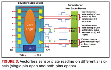
The challenge. High-speed differential signals, commonly known as SerDes (serial/deserializer) are reason to remove testpoints on assemblies. ICT has seen innovations to regain test coverage on connectors and devices connected to boundary scan devices without the need for testpoints by using a combination of boundary scan devices as signal driver and a noncontact signal sensing or vectorless sensor plate to detect opens and shorts on connectors, sockets and semiconductor device pins. However, this solution still falls short of being able to provide 100% coverage on differential signals. An example of failure escaping detection is when both differential signals (Tx+ and Tx-) are open, but the detected measured value of vectorless sensor plate will still be the same when both signal pins are properly soldered (Figure 3).
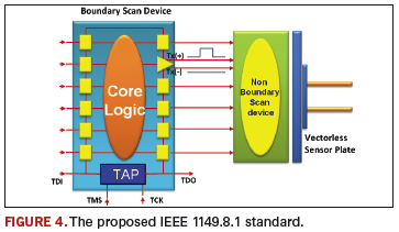
The proposed solution. IEEE 1149.8.1 entails a selective AC stimulus or differential signals, which when combined with noncontact signal sensing or a vectorless sensor plate, will allow testing of the connections between devices that adhere to this standard and circuitry elements such as series components, sockets, connectors and semiconductor devices that do not implement IEEE 1149.1 standards.
This standard specifies extensions to IEEE 1149.1 that define the boundary-scan structures and methods required to facilitate boundary scan-based stimulus of interconnections to passive and/or active components. This standard also specifies Boundary Scan Description Language (BSDL) extensions to IEEE Standard 1149.1 required to describe and support the new structures and methods (Figure 4).
The benefit. IEEE 1149.8.1 would enable selective AC stimulus generation that, when combined with noncontact signal sensing, would allow testing of signal paths between devices adhering to this standard and passive and/or active components. The biggest benefit of 1149.8.1 is that there is already a working solution currently implemented in some ICTs using a noncontact signal sensing or vectorless sensor plate that detects open/shorted pins on non-boundary scan devices and connectors connected to boundary scan devices.
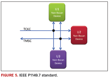
IEEE 1149.7
The challenge. Assemblies, especially those used in consumer products, are pressured by shrinking form factors. In recent years, we have seen implementation of multi-core system-on-chip (SoC), multi-die packages on system-on-package (SoP), and package-on-package (PoP) devices. All these technologies pose new challenges when it comes to manufacturing test due to limited testpoints and higher speed. This is causing existing manufacturing test systems to lose test coverage, even with the implementation of IEEE 1149.1.
The proposed solution. IEEE 1149.7, also known as compact JTAG or cJTAG, is compatible with the traditional IEEE 1149.1 (JTAG) standard to provide an enhanced test and debug standard that meets the demands of modern systems. One unique feature of 1149.7 is the reduced pin count interface for the test access port (TAP) interface; it uses a two-wire interface, versus the traditional 1149.1 four- or five-wire TAP interface. Since IEEE 1149.7 is compatible with 1149.1, this proposed standard also permits four- or five-wire implementation (Figure 5).
With the adoption of a two-wire interface on IEEE 1149.7, devices on the IEEE 1149.1 standard will benefit from this, as it makes it easier for boundary scan to be implemented on complicated new package technologies such as SoC, SoP and PoP, which does not implement 1149.1 boundary scan chain using the standard four or five-wire TAP interface.
The benefits. IEEE 1149.7 would enable easier implementation of IEEE 1149.1 for SoC, SiP and PoP. IEEE 1149.1 implementation is limited to boundary scan chains, as it requires the connection of every TAP interface of every boundary scan device targeted for testing. In comparison, IEEE 1149.7 would simplify this by enabling a star architecture (Figure 5) more appropriate for SoCs, SiPs and PoPs. When used on SoCs, 1149.7 would enable testing and debugging of each core or chip in the package, using boundary scan in a single 1149.7 two-wire interface. This implementation is also possible on multi-die SiPs or PoPs. A key advantage of 1149.7 is that it can be implemented on through-silicon vias that would link each die through a via that connects the 1149.7 interface on each die to one another. How successfully these proposed standards are adopted on the manufacturing floor depends on how well they will fit into the existing manufacturing test systems such as ICT, manufacturing defect analyzers and functional testers without impacting throughput, and while regaining maximum test coverage no longer available on the older testers. Another important factor will be the cost of the tools and their implementation.
Bibliography
1. Bill Eklow and Ben Bennetts, IEEE P1687 (IJTAG) Draft Standard for Access and Control of Instrumentation Embedded Within a Semiconductor Device, ETS 2006 embedded tutorial. 2. IEEE P1687 Working Group, http://grouper.ieee.org/groups/1687/. 3. IEEE P1581 Working Group, http://grouper.ieee.org/groups/1581/. 4. P1581 Working Group, “An Economical Alternative to Boundary Scan in Memory Devices,” January 2007. 5. IEEE 1149.8.1 Working Group, http://grouper.ieee.org/groups/atoggle/. 6. Adam Ley, “New 1149.7 Enhances 1149.1 Test Access Port, Maintains Compatibility for Boundary Scan,” Asset Connect, 2009.
There is a practical way to sequentially implement the two efficiency systems.
There is no debate that correctly applied Lean manufacturing philosophies can increase production efficiency. However, there are variations in Lean tools. The fundamental difference between Lean and Lean Sigma is that while Lean manufacturing focuses on the elimination of waste by removing steps in processes, Six Sigma fine-tunes processes by focusing on specific process improvement activities.
Implement core Lean philosophy first. EPIC chose to implement Lean manufacturing principles first. Major points of focus included:
Process flexibility. A critical first step was developing a production process that could handle small lot sizes over a wide range of customers and product types. This included working with suppliers capable of modifying their equipment to support rapid changeovers.
Operator cross-training. Operators are cross-trained in several production processes and certified to a range of skills in a training matrix. Compensation is tied to certification levels achieved. A core group of operators is deployed in a range of critical production processes and moved throughout the factory based on areas of highest demand.
Visible/frequent communication. Visible scheduling tools are used to ensure that scheduling data are in the hands of those charged with producing products. EPIC uses a three-zone system for production staging and a two-bin system for material planning. There are no production schedulers. Operators are empowered to prioritize the production sequences for each line based on color-coded pull signals. Material use is coordinated electronically between facilities via a bar-coded “virtual” Kanban planning system that mirrors the “visual” card system on the factory floor.
Visible metrics. A Plant Operating Review (POR) system drives the monitoring of approximately 50 metrics company-wide down to the floor level. These metrics are reviewed on a daily/weekly basis by the customer focus teams, monthly by the plant managers and directors of operations, and quarterly by the senior management team.
Mutually beneficial supplier relationships. We use a combination of supplier education, internal planning tools, excellent communication, and strong working relationships with customers and suppliers to help motivate suppliers to support Lean principles.
Six Sigma as an enhancement tool. Six Sigma principles are incorporated in an enhanced, disciplined analytical approach.
EPIC’s in-house reliability laboratory supported new process definition and validation; new product process validation; and resolved internal, supplier and customer quality issues prior to implementation of Six Sigma tools. Six Sigma’s Define, Measure, Analyze, Improve, Control (DMAIC) approach has now been implemented to enhance design for manufacturing/testability (DfM/DfT) analysis, process improvement and/or corrective action effort.
We have three Black Belts and are in a second wave of Green Belt training. The Six Sigma focus has been on scrap and defect reduction. As focus areas are identified, the appropriate project engineer is given the training, tools and mentoring to analyze the project selected for improvement. These improvement projects use the DMAIC approach.
In the Define phase, participants validate that this is a good project, define the improvement goal and define the team and team leader.
In the Measure phase, the real project work starts. Past performance is measured. Pareto charts and process mapping are utilized to determine the high hitters in terms of defects. The measurement system is validated using a gauge R&R tool, since decisions will be based on the data collected. Typically, an experiment is set up where several people are surveyed using several boards to determine whether an induced defect is the defect that everyone recognizes. This statistical tool measures whether the defect assessment is consistent across people or machines.
The Analyze phase focuses on the critical few areas identified to determine root cause of those defects. A cause-and-effect diagram (also called the fishbone diagram) is used. The team conducts a brainstorming session and then tests its hypothesis. Any variances are analyzed. The team also tries to estimate the impact of an input variable, such as raw material, temperature or line speed, on a machine to the output factor to determine which change has the most impact. In the Improvement phase, there is evidence of problem root cause. The team develops an action item list to identify what needs to be changed and when it will be changed. The recommendations are then validated.
The Control phase ensures the output continues to be monitored to guarantee the corrective action in input variables stays in place. Any changes are documented. This ensures consistency and documentation of institutional knowledge. Any cost savings is measured.
One recent project involved a goal to reduce scrap from 1.1% to 0.8%. It was determined that the root cause was illumination values that were causing misaligned placement against the pads on certain BGAs and ICs. To improve the parameters, the team used design of experiments to determine the best illumination parameters by shape of components. It then analyzed manufacturer recommendations and experimented with a range of values to get the best results. Once the results were validated, it made the best combination of values the default in all machines. Because we use a standardized SMT placement platform across the company, this fix has been implemented in all facilities.
The board being analyzed has gone from a 1.1% scrap rate to 0.77%.
Many gold failures are incorrectly attributed to black pad issues.
Figure 1 shows the surface of a nickel pad on a printed board after stripping the gold from the nickel surface. The image shows limited evidence of corrosion on the nickel surface at the grain boundaries on a bare board. Some evidence of gold is also still visible. Solder joint failures when examined normally show far more corrosion around the nickel boundary. Much debate centers around the subject of black pad. Changes to nickel chemistry and better control have reduced solder joint failures.
Unfortunately, many gold failures are attributed to black pad issues, when clearly they are not. Close cooperation is necessary with the PCB supplier and its chemistry supplier to determine the cause of the problem. Always ask to review the chemistry supplier’s audit reports conducted at the PCB supplier’s offices. Independent analysis also may be required, if the assembly processes are considered the root cause of any joint failure. Review the PCB fabrication process, the reflow temperature and time in a liquid state for the solder paste.
These are typical defects shown in the National Physical Laboratory’s interactive assembly and soldering defects database. The database (http://defectsdatabase.npl.co.uk), available to all this publication’s readers, allows engineers to search and view countless defects and solutions, or to submit defects online.
Positioning CSPs and noise-sensitive devices are two of a host of considerations.
Effective, accurate component placement takes into account the best practices of design and assembly, both of them inextricably intertwined. The layout engineer must take special care to correctly place components on the board, since this has a direct bearing on assembly and testability.
Also, with the evolution of various technologies, assembly takes on newer meanings, dimensions, and demands. In particular, use of fine-pitch BGAs is escalating, challenging current assembly practices and procedures. In these situations, PCB design and assembly know-how and experience are the linchpins for effective placement.
Design for assembly takes into account such factors as through-hole versus surface mount components, critical ribbon and cable assemblies, cutouts, vias, decoupling capacitor placement, mechanical aspects, and others. Through-hole technology has become more of a specialty, while surface mount is the basis for most of today’s designs.
In terms of placement and routing, the beauty of an SMT design is its superior leverage relative to board’s real estate area, because both sides of a board can be utilized. This creates certain challenges, however. For instance, an experienced PCB designer doesn’t want to place a noise-generating device or high–frequency, sensitive device close to the clock where the signal will incur interference. Improper component placement raises the probability of high-level noise and an unacceptable signal-to-noise (SNR) ratio.
Through-hole mostly is used for connectors and mostly is limited to signals coming into and exiting the PCB. However, SMT connectors increasingly are used. But some applications employ a combination of surface mount and PTH components. When a PTH connector is used, another component cannot be placed on the other side of the board since there’s no usable real estate.
The advantage of a surface mount connector is both sides can be used for component placement. However, the PCB designer must take precautions when placing either PTH or SMT I/O components. The same concepts apply to other components with gold fingers, ribbons, or cables attached to the board. Usually, the physical location of these devices is fixed. For example, a gold finger of a daughtercard going into a motherboard needs to be at a certain location to ensure a proper fit. At the same time, the board designer must ensure space limitations are not violated and no mechanical, vibration, or height-related issues are created due to that particular placement.
The designer also must check that all X and Y coordinate calculations are accurate. This means the cutout or gold finger is made at the right location because if a hole is off by, say, 0.010˝ to 0.020˝, then a pre-selected cable will not go in the right place. Physical location and dimension calculations cannot be fudged if I/O components are to precisely communicate with fixed devices from other systems or subsystems to the PCB.
As for vias, there are an array of types, including blind, buried, stacked, and through-hole vias. A through-hole via goes from one side of the board to the other. Blind vias go from an outerlayer to a middle layer; for example, a blind via originates at the top layer and terminates at one of the innerlayers. Buried vias originate and terminate within innerlayers. Stacked vias originate from each of the outerlayers and terminate on the innerlayers at the identical location.
When it comes to selecting vias for accurate component placement, the designer must consider the pros and cons of each to avoid assembly issues later. For example, for smaller and handheld devices, which are compact in terms of available real estate, there is sometimes no choice but to use blind or buried vias. These particular vias are difficult to fabricate and increase manufacturing cost. The advantage of these vias is that routing and connections use the innerlayers, thereby saving top and bottom layers for component placement and critical routing.
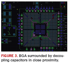
Signal integrity is another major DfA aspect when it comes to component placement. It is critical to appropriately place bypass capacitors next to BGAs, CSPs or QFNs. This is especially true in high-speed designs, for which transmit and receive paths must be highly accurate and extremely short, to avoid impedance control issues. The signal from a BGA ball to a bypass capacitor must be cleanly filtered to suppress noises, hence the importance of maintaining close proximity and placement of these capacitors next to BGA, CSPs and QFNs.
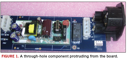
If the board has too many components close to the edge and protruding from the board (Figure 1), it’s best to use tab and route, versus scoring during board fabrication. By using tab and route, there is a small portion of rail to separate two boards from each other. On the other hand, a scoring device separates boards next to each other and is not ideally suited for boards with protruding devices.
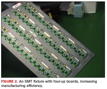
Also, for efficient assembly involving small board sizes that are panelized, create accurate fixtures for handling PCBs during reflow soldering. But a panel must not be made too large; optimal panel size must be calculated to maximize manufacturing efficiencies. Otherwise, the board could warp from the component weight. Aside from proper assembly techniques, DfA compliance also deals with different tools and the point to deploy them during assembly. For instance, will x-ray be applied as a process check at the end of each board or for sampling one of every five, 10, or 20 boards? When will a certain fixture be used? During surface mount? Wave solder? Or maybe at AOI or testing? These issues need to be addressed at the planning stage, when the CAM engineering/planning department is reviewing the data and preparing the processes and visual aids for the jobs.
Not all machines will be able to use the same fixture, due to varying dimensions. But they will be different because they’re created to conform to different board sizes. Moreover, they have their own mechanical and tolerance limitations. Be aware of these tolerances, as a universal fixture is not a cure-all. At times, there must be multiple fixtures, one for SMT (Figure 2), another for wave solder, and still another for testing. Most often this occurs when boards are smaller and not uniform. For example, they may be semi-circular, round, half moon or L-shaped. In these cases, various types of fixtures are used to make assembly an easy, reliable and repeatable process.
As far as BGAs are concerned, they demand special scrutiny and attention. BGAs require just the right amount of solder paste. Too much could cause shorts between the balls. Then there’s no choice except to depopulate and re-ball it, or use a new BGA device. Moreover, it’s important to ensure correct placement, keeping in mind component orientations and polarities. When rework is involved, sometimes it is important to desolder the nearby decoupling capacitors (Figure 3) or other devices, making rework possible.
Also, BGAs should never be placed close to the board’s edge. Reason: A BGA needs a peripheral area that’s heated during rework. If close to the edge, then that half side close to the edge will not sufficiently heat, simply because there’s no mass around the BGA device to heat. Hence, the BGA will be extremely difficult to depopulate.
At the stencil design stage, sound assembly practices depend on the decisions over foil thickness, stencil frames, aperture to pad ratio, for dispensing correct amounts of solder paste, when to use window panes, performing first article inspection, and the right type of solder paste, along with use of paste height measurement systems.
Foil thickness determines the amount of paste to be dispensed. Assembly personnel must determine whether a stencil will be 0.04˝, 0.06˝ or 0.08˝ thick to gauge the amount of paste required. As foil thickness changes, it changes the amount of paste dispensed on pads, thereby affecting the thermal profile. Foil should come framed from a vendor. Stencil foils without frames create time and reliability issues. Time-consuming mistakes may include mounting the foil upside down or in reverse, and damaging it. Also, when stencil foils are not stretched properly when mounted on the adapter, it can adversely affect the quality of the paste deposit, causing bridging and misregistration on the SMT pads.
Aperture-to-pad ratio decisions, for example, can be whether those ratios will be 1:1, 1.1:1 or 0.9:1. The ratio 1:1 means size of the stencil opening is equal to the SMT pad. A 0.9:1 ratio means the size of the stencil opening is smaller than the SMT pad, thereby dispensing smaller amounts of paste. This mostly is used in ultra-fine-pitch SMT applications.
Sometimes a stencil opening is made a bit larger compared to the pad size so that the aperture to pad ratio becomes 1.1:1. This permits slightly more paste to be dispensed on the stencil. This is mostly used in heavy analog applications. In each case, assembly personnel must be fully aware of a board’s end application and whether the dispensed solder paste is adequate. Some studies have found as much as 75% of defects are related to paste dispensing, which bears directly on stencil design.
Window panes are implemented when there is a huge opening on a stencil design. Consider a 0.5˝ x 0.25˝ opening, which is extremely large when it comes to dispensing paste. Therefore, a decision is made to pane the window to create smaller window or opening sizes within the large opening. For example, six different slots or panes may be created to control the amount of paste going to these different panes versus applying a whole blob of paste on the pad.
Also, every time a decision is made involving stencil design, it’s vital to perform a first-article check to ensure the proper amount of paste is dispensed, or whether another foil needs to be cut due to a thickness or aperture-to-pad ratio change. This would act as a process verification tool for dispensing the right amount of paste on the pads.
Here’s where a first-article inspection system proves invaluable. FAI systems are relatively new. They help create the first-article board by scanning the image of the whole board (the golden board), and comparing the images of all other boards with this golden board to ensure all components are placed properly, with correct orientation and polarities. It is used as a process verification and inspection tool to significantly reduce the human interface and make inspection and QC more reliable, repeatable, and faster by at least 30 to 50%.
Last, solder paste and its varieties are vital considerations for accurate component placement. Normally, Type 2 and 3 solder pastes are used for analog devices and analog/digital. Sometimes Type 4 (or finer) is required for fine-pitch BGAs, CSPs, and QFNs.
Generally speaking, solder paste is a mix of metal grains and certain chemicals in a format conducive for soldering. Those metals are of considerably finer grain in Type 4 compared to Type 3. This means Type 4 can be used more accurately for fine-pitch components because its tolerance is slightly higher compared to Types 2 and 3. Viscosity for Type 4 is finer. This means grain particles are joined tighter together compared to those of Type 3, and thus can be used more accurately for fine-pitch components.