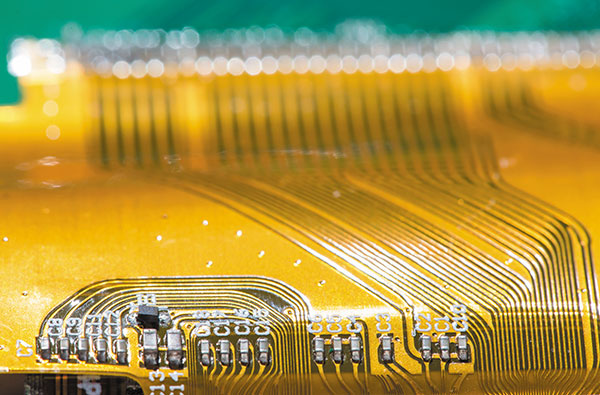
When designing a rigid-flex, start with flex in the middle of a stack-up and move outward.
You’re designing a new rigid-flex. Devices are getting fanned out, via structures defined, and layer count is becoming clearer. You have determined how many flex layers you need from rigid section to rigid section. There are competing considerations on how those flex layers are configured: foil and dielectric thickness, bonded or unbonded, and where they will be in the stack-up of layers. All this impacts flexibility and how the part will bend in the installed application.
For today, let’s concentrate on where the flex layers land in the stack-up and the effect that can have on manufacturing and end-application use. Several strategies have rational logic and can be successful in select situations.
The most common and lowest impact is to place the flex at the middle of the stack-up. There are several advantages. First, it permits symmetry of the stack-up. Symmetry provides the opportunity for the flattest stack-up with the least tendency for bow and twist. This is more and more critical as component pitches get denser, and the size of BGAs and FPGAs gets larger. This is also the easiest to fabricate with the lowest cycle time, resulting in the lowest cost. If you can put the flex in the middle of the stack-up, this is the best option.
Increasing distances between rigid areas helps prevent potential damage.
When designing a rigid-flex that needs to bend 90° in the flex area, what is the minimum flex length (distance between rigid sections) one should allow?
That is a loaded question without knowing the overall thickness and width of the flex layers. For this column, I will assume only a couple of flex layers, and the flex width is 2" or less. Several issues come into play when determining the minimum distance between rigid areas on a rigid-flex. Some will affect the supplier’s cost because of yield reductions, and others may affect the mechanical function.
Manufacturing issues. Fabricating a rigid-flex circuit means juggling a number of technical issues to get everything to work. First, the rigid material must be removable in the flexing areas. (The rigid material is applied in full sheets.) This can be done by pre-scoring the rigid-flex interface lines part way through and removing the adhesive in the flex areas used to bond the rigid material to the stack.
The updated rigid-flex specification overhauls copper thickness requirements.
As we start a new year, it’s a good time to review what changed in 2021. In the flex world, the IPC Flexible Circuits Performance Subcommittee worked through the pandemic and released a new revision to IPC-6013. Revision E was released in September, replacing an amended Revision D from April 2018. Some updates and changes are subtle, while others are significant. Many changes attempt to increase clarity.
Let’s start at the finish – final finish, that is. Tin, silver, and ENIG/ENEPIG will not have minimum thicknesses in IPC-6013. Instead, we are defaulting to the new IPC-4552/4553/4554/4556 specs for thickness and sampling frequency. This avoids unintended differences or conflicts as the finish specs are updated.
Often questions arise related to the rigid-to-flex transition – and what is delamination versus non-lamination? In paragraph 3.3.1.3, we added an explanation about what’s happening at the transition and a new Figure 3-1B to provide a more visual explanation of what is acceptable and rejectable.
Flex circuits have always been more prone to questions about foreign material or entrapped particles. Unlike rigid boards, flex circuits are more transparent, making cosmetic anomalies more evident. Once noticed, disposition is required. We expanded Section 3.3.2.4 to provide more clarity on acceptability, including prepreg resin that may deposit on the external surfaces of flex regions of rigid-flex.
Changes are often made to the spec based on input or questions from users. The team received questions about what holes should be evaluated for hole pattern accuracy. Some questioned the need to inspect all hole locations, especially interconnect vias, which do not have components attached. Most drawings do not have all holes physically dimensioned, relying solely on the CAD data file. Moreover, annular ring requirements control hole locations. We added clarifying verbiage in paragraph 3.4.1 indicating only those holes specifically dimensioned on the drawing itself should be inspected for pattern accuracy.
IPC has always required fillets at the pad/trace junction for Class 1 and 2 designs. If they did not exist or were not allowed, it was implied Class 3 annular ring was required. To be more direct, we added to paragraph 3.4.2 explicitly requiring 0.001" minimum annular ring if no fillets are present.
HDI features within rigid-flex products have been rapidly adopted and include employing blind vias and microvias. Often these vias are “via-in-pad plated over,” meaning the via is in the middle of an SMT pad. Questions related to the inevitable dimple or bump created by this via included, “Was it rejectable like any surface anomaly in the pristine area of an SMT pad?” We modified the overall requirement for anomalies in the pristine area to limit the dimple or protrusion vertical dimension to match the dimple protrusion requirement for filled vias.
In the same vein of HDI features, if microvias or blind vias are on both top and bottom layers of a board, thermal stress coupons must reflect these via structures; we included this language in the specification. In addition, both the top and bottom via structures must be directly exposed to the solder. This may result in testing extra coupons to accommodate this requirement.
Another IPC activity across multiple specifications attempts to discern between dewetting and the natural high/low variations in the hot air solder and solder reflow processes. In hot air solder leveling (HASL), it is common to see solder pooled up toward the trailing edge of the pads. This is a mechanical issue caused by the air knife blowing the solder to one end of a pad. In addition, surface tension of solder tends to cause mounding of the solder. The following note has been added to IPC-6013 (and will be added to IPC-6012 and J-STD-003): This thickness variation is a natural occurrence and is not rejectable.
An attempt was made to clarify maximum copper plating wicking condition in a plated through-hole. Wicking occurs when the copper plating “wicks” down the glass weave bundles in areas where the resin is removed or is not intimately joined to the glass. There has been confusion between etchback, wicking and a combination of the two attributes. While the new wording is improved, it is still not clear enough. The IPC team stepped back and created a tiger team to revise this topic in its entirety. Stay tuned for a complete rework of the etchback and wicking requirements in IPC-6012 and -6013, either in the next revision or an amendment in the near future.
FIGURE 1.If there is a specific minimum thickness of copper on certain layers, explicitly state it on the drawing to ensure it is accounted for.
Probably the biggest change was an overhaul of the copper thickness requirements after processing. After much discussion, debate, and finally consensus, the entire section was rebuilt:
It differentiates between unplated and plated internal layers, as well as external plated layers.
The new requirement permits more reduction of the initial base foil, provided the total copper thickness requirement is met after plating.
For button-plated designs, it clarifies copper thickness outside the button area to meet the internal layer foil requirements, not the external (plated) requirement.
Absence of copper at the knee of the hole may be acceptable if other requirements are met.
The thickness table was simplified by eliminating columns.
Much of the discussion related to this section revolved around assumptions and expectations. Given the wide spectrum of via structures and plating and planarizing processes, it is not prudent for designers to assume a certain minimum thickness of copper on any given layer. If a designer has a true need for a specific minimum thickness of copper on certain layers, it is recommended to explicitly state it on the drawing to ensure it is accounted for.
IPC-6013E includes other changes too. Any section that has been changed is highlighted in gray to alert the user.
Changes to the specifications are truly user- and supplier-initiated. Input from members is how we refine and update the specifications. Participation in the process is encouraged. The industry wins when you volunteer, as it helps bring needed changes to specifications. You win as a volunteer, as you get a better understanding of the specifications and build a healthy network of industry experts you can leverage throughout your career.
NICK KOOP is director of flex technology at TTM Technologies (ttm.com), vice chairman of the IPC Flexible Circuits Committee and co-chair of the IPC-6013 Qualification and Performance Specification for Flexible Printed Boards Subcommittee; This email address is being protected from spambots. You need JavaScript enabled to view it.. He and co-“Flexpert” mark finstad Mark Finstad (This email address is being protected from spambots. You need JavaScript enabled to view it.) will speak at PCB East in April.
“I am developing a flexible circuit for my application and will soon be ready for prototypes, followed by production a few months later. A lot of flexible circuit suppliers are out there. How do I know if a vendor is reputable and will meet my needs?”
Many variables must be considered when picking a flexible circuit supplier. Do your homework and find a vendor that is a good fit for the project. It is advisable to also select a vendor that will support your program from prototype through production. Multiple vendors could build to the same Gerber files and overall specifications, but the end-product could have differences due to processing and material variations between suppliers. Switching fabricators midstream can introduce significant risk at a critical time between prototype and production. Following are the items I recommend learning about a vendor before making your sourcing decision:
Circuit application/performance class. This is more about the IPC performance class rather than specific application, but mil-aero, implantable medical devices, and so on generally are specified as IPC Class 3, while most everything else is Class 2. IPC Class 3 is the highest reliability and overall performance class and is usually specified when the product is used in a life-critical application. Class 3 product typically requires more stringent processing controls, QA, and documentation. Suppliers that primarily serve Class 3 users typically “stay in their lane” and build all products to Class 3 performance level regardless of the requirement.
To continue reading, please log in or register using the link in the upper right corner of the page.