 Overcoming “anywhere but here.”
As the devices shrink in pitch and increase in pin count, current density becomes a concern. The outer rows of devices typically have lots of signal pins, while center pins focus on power and ground. This situation means that designers must reserve the first few layers of the board specifically for fan-out (Figure 1).
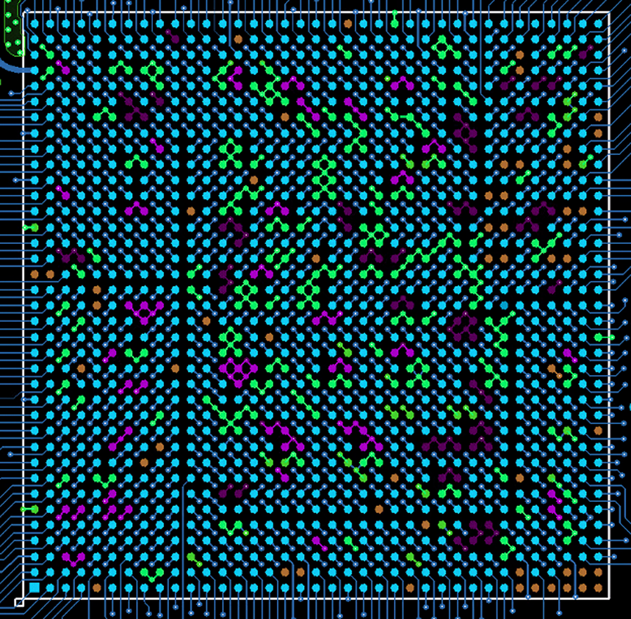
Figure 1. Just your average 1,369 pin FPGA using a 1.27mm (0.05”) pitch. In terms of colors, green indicates the primary ground domain. Deep purple represents where heavy metal is desired for high current. The lighter magenta is a lower wattage, more spacey kind of metal (like Pink Floyd). Orange marks the no-connect pins.
One of the worst mistakes when dealing with a BGA of 1,000 pins is to drop a via deep into the board for pins on the device’s edge. Be ready to use every lane of the first three layers, and route layer 2 through the air gaps between the other two.
The point is to get away from the device until the trace gets a chance to join the normal flow of the routing channels. You have two distinct areas: the fan-out zone and everything else, where routing up, down, left and right makes sense (Figure 2).

Figure 2. The first thing is to address the outer ring(s) where the top layer is used to escape to a via for the internal routing layer or to a nearby component that is placed there for that reason. The arrows indicate the fan-out flow, always away from the core. For the sake of rework (and room for the fan-out), a component-free area around the device will make it easier to desolder if it needs to be replaced. Otherwise, the tech has to remove the nearby components first.
Find your beach and drop a via that takes you to a level where the current is going your way. Until the vast majority of connections are handled that way, routing between component clusters makes no sense. Fan-out is early in the timeline and updates to the schematic are probably on the table. It’s much easier to move or edit a group while isolated from the rest of the board.
Route the outer ring of pins to “anywhere but here” using the outer layer of the board. If space permits routing between the pins, then the second ring of pins should also escape on the outer layer. If there is no room for that, like with a 0.4mm pitch, then the next layer down is the best option, even if it’s the traditional ground layer.
Conventional wisdom suggest routing orthogonal to traces on the adjacent layers. In reality, that’s a nonstarter on the edges of a pin field. The right routing direction radiates far enough away from the center of the device to connect to components placed around it or to a via where we can start adhering to regular routing according to each layer’s purposes.

Figure 3. This trace in red is eating too many vertical routing channels. One option is to drop a via in the upper left corner and wrap around the differential pairs on the horizontal routing layer. The other option is to use the same brown layer all the way and follow the arrows on the right, routing under the FPGA to the point where only two traces pass through the fan-out vias. From there, routing goes all the way around the high-speed lanes. The first option seems like less work.

Figure 4. The strategy around horizontal and vertical routing layers is knowing when to break away from the trend. The little box full of dangling lines has enough lanes to proceed with a minor revision to the trace. Obstacles such as shields, slots and board edges can be a place to route counter to the prevailing directions as a matter of necessity.
If a PMIC device has external oscillator pins, they are likely buried deep inside the BGA pin field rather than on the perimeter where we like them. Are you going to have headroom for a crystal on the far side of the board? Some internal routing might be involved in getting to the crystal.
In that case, I recommend using a guard band around those traces. Like almost every other component, placing the PMIC near the SoC makes sense. This practice minimizes signal degradation, similar to how engineers position a single regulator near the pins that use the power supplied to any chip. In the case of a PMIC, such concerns are numerous.
With the power domains and essential routing behind us, we can finally close the schematic and play connect the dots using the two innerlayers for vertical and horizontal routing lanes. The unrouted segments have no remaining length or width requirements. My guess is the average person would think this is the nature of most, if not all, routing solutions. This belief has become less common as the percentage of constrained nets has grown over time.

Figure 5. Both power domains can be connected without overlap. If it weren’t obvious before, it’s now clear we can supply the two main power domains with shapes on this layer based on the routing study. The shapes will fill in to distribute the voltages with minimal neck-down. (As we would most likely be using dynamic copper for the power planes, the traces would remain as a backbone. Although they are not close to sufficient in terms of width, they will prevent a future trace from splitting the plane entirely, in case additional routing ends up on this layer.)
Closing those last traces can be a chore as all the good routing channels seem taken. Sometimes, the routing goal becomes “anywhere but here.” You might start at both ends and route a meander as far as it goes in any direction. Along the way, you might have to be “impolite” with the existing work. If the two ends can cross each other at some point, then the routing solution is only a via away. On a 95%-routed board, that still may be a problem. I remember spending 20 minutes clearing out space to add one ground via. Such is life under an NFC chip of a phone.
The fan-out is a chance to make minor adjustments to the placement. This effort continues throughout the fan-out and routing steps. There’s always some guesswork as we go about making design decisions. We’re not always right, but we’re always ready to make it right when new information comes to light.

Figure 6. Re-examining this unused MIPI corner getting two more vias out of the grid. If only one trace may be routed between pins/vias, ensure you do just that. Get a trace through every gap. We can depressurize inner layers in the same way. This applies to pin grid connectors as well as BGA devices. Maximizing each layer’s number of connections is how layer count is reduced to something more feasible.
Preliminary routing. Cross-probing and selectively displaying or colorizing nets provide insight into what’s to come. Although we’ve checked off on the placement gate, it’s a good idea to maintain elasticity for as long as possible. Modularity proves useful when the inevitable update makes it necessary to relocate or rotate a device and its constituent parts.
That said, we must begin connecting the various devices at some point. The heaviest hitting device on the board is a good place to start. It could be key because it uses the most power or has the most interconnects. It may also be the main amplifier or whatever motivates the product. Every board has a device at its heart, so that’s where risk management begins. We must start somewhere.
Step one is the highest priority net on the highest priority chip. It will all be downhill from there; working toward the least significant connections. Operationally, I might not even place pull-up resistors until I complete the pin-escape from the device. Once the trace is fanned out and routed to a clear spot for the via, land the low priority part can land. The same can be said for test points. Get away from the dense area and find a home for the test point.

Figure 7. At times, everything else must step aside and clear all layers for a printed antenna. I use a net short property to tie the antenna shape and the ground via so that the two can coexist at DC and the antenna’s frequency. Like most of these slides, this is made entirely from scratch. The takeaway: Ground vias are always in demand around features like this one.
Like going back to the good old days, we’re using the organic, free-range kind of intelligence that comes straight from our brains. Sometimes it helps to flip the bit. Mirror the board’s image. Soften the color palette. Make it easy on yourself. I hope many of you remain blessed with the option to work from home.
Either way, consider via stubs when doing the fan-out. If the chip is on layer one, then you should use the higher layer numbers for diff-pairs and similar routing. If the route is on layer 3, a stub will run from 3 to the bottom. Avoid back-drilling whenever possible, as it can become a signal integrity thing as layer count increases.
John Burkhert, Jr. is a principle PCB designer in retirement. For the past several years, he has been sharing what he has learned for the sake of helping fresh and ambitious PCB designers. The knowledge is passed along through stories and lessons learned from three decades of design, including the most basic one-layer board up to the high-reliability rigid-flex HDI designs for aerospace and military applications. His well-earned free time is spent on a bike, or with a mic doing a karaoke jam.


