The quarantine may have created the biggest shift in how PCB design works.
 As a career PCB designer, I’ve seen a lot of waves break over the electronics industry, but not since the very foundation of electronic computer aided design (ECAD) have I seen such a significant paradigm shift in our work practices. From the mid-20th century onward, computers have become involved with our design efforts. Aerospace and automotive industries led the way along with universities; about the only places where computers were available in those days.
I went to school for this in 1988, the year the telephone system moved from Alexander Graham Bell’s analog technology to a digital system. Four years prior, the US Congress used antitrust law to break up AT&T into numerous regional “Baby Bells.” This set off the telecom revolution that led us to today’s information saturation.
The first wave of PCs. Back then, the “Big Three” service providers were Compuserve, Prodigy and AOL. Prior to that were so-called Bulletin Board Systems (BBS) where my primitive computer could connect over the old phone system at baud rates that would be laughable in today’s world. Let’s just say that 56K dialup would have been crazy talk.
The computer had no hard drive, only a pair of floppy drives. They weren’t the 1.4MB kind either. The OS actually ran on one of the 360KB floppy disks. A piece of connectivity software called X-Modem ran in the other slot and allowed me to specify such things as the number of bits, (8) whether to use a stop bit (yes), whether to have duplexing (full) and finally whether to use odd, even or no parity (even).
The sound of a “dial up” session – that series of various beeps when the two machines connect over phone lines – is an audible manifestation of the two devices agreeing on a protocol. If the wrong parameters were entered for the host device, then the text on the screen would be garbled. Imagine if the “internet” were some fellow who had a total of eight telephone lines running to his house. That’s how many of us could be online at a given time. Good thing the ol’ computer had redial.
The day when that computer became obsolete due to the rise of the big three was the second time PCB design underwent such a significant sea change. The digital revolution was on. Winners in the portable computer market would be sorted out in the field of innovation. Battles played out over such things as battery life, screen resolution and megabytes of double data rate random access memory (DDR) that could be listed on the marketing material.
The effect on PCB design, with regard to the available software, was the ability to assign multiple nets to a bus and generate sets of rules regarding those groups of nets. We had to design the machines that helped us design even more machines. Graphics support went from that text-only display screen to ever more vivid imagery driven by, of all things, gamers. The wider graphics pipelines required more out of the central processors, which started adding pins while decreasing their sizes.
Computers hit the road. Meanwhile, the mobile revolution was setting up to be the next game changer. No longer tethered, mere conversations gave way to texting, and even sharing a picture or two. South Korea was ripe for cellular technology, primarily because it had very little in the way of telephone wires out in the rugged countryside.
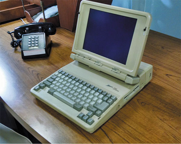
Figure 1. A little more modern than my first laptop, this Zenith unit is aboard the museum Battleship Missouri in Pearl Harbor.
Cellular towers made a lot of sense for their country, but they also traveled well. When Qualcomm, which started the 3G cell tower business, sold it to a company in Finland, my company made the pivot to South Korea, which had collectively decided to become an exporter.
Time marched on and cellphones became smartphones by combining as many features as possible under the screen. Of course, the largest feature was the battery, because, as with the personal computer, a technology race was on and run-time was one of the battleground metrics.
Then it was time for PCB designers to start thinking small. Mobile devices for the consumer market gained a focus on thin and light in addition to durable and powerful. Miniaturization brought the microvia and all the stack-up conditions that apply to sequential lamination. Managing core vias with just one central via is difficult on its own.
The way I see it, a few watershed moments have altered the course of PCB design history.
- Going digital, using computers to design better computers.
- Computers becoming more connected to each other. Edge routers and other infrastructure were needed, and layer counts went up.
- Computing going mobile and shrinking the playing field. Chips and boards became smaller, faster, and more efficient, and board technology had to keep pace with the ever-tightening geometry, while upping the importance of SI/PI issues.
- Being able to work from anywhere without the boundaries of space and time.
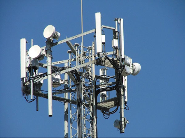
Figure 2. Cell towers flourished like dandelions as we all became more connected to each other and then to our shared data.
This last point is unlike the others in that it wasn’t so much a technological breakthrough but rather a societal imperative that made it happen. I would point back to the trust busters of 1984 as the closest parallel in this regard.
Office space: not what it used to be. Over the years, tech companies have consolidated around the idea of desks lined up in rows rather than separated by cubicles or actual walls. In every case, the bulk of our jobs took place on the monitors. Kickoff meetings and design reviews found themselves in a dedicated room.
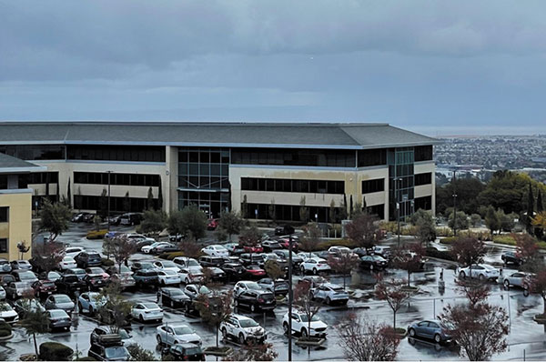
Figure 3. Office, sweet office? The GoPro headquarters is what you’d expect, so I go there once a week by choice.
The meeting rooms themselves were adapted ahead of the quarantine to include large wall monitors. This allowed people from other buildings around the campus to join remotely. I can recall the meetings of the Xbox design team prior to all of this where most of the people in the meeting were not actually in the room. I came into the office every day but was lucky if I saw my manager twice a week.
That turned out to be good training for what was to come. All the pieces finally came together. Portable computers with enough power, fast and secure connections, and software geared toward online collaboration have coalesced around the global pandemic to kickstart a process that has proven rather successful. It would be difficult to put that genie back in the bottle.
The upshot is that I could, in theory, move to Colorado and take my job with me. Conversely, I could accept an offer in Colorado and not have to move if that was my desire. This opens pretty much all the job opportunities regardless of location. Don’t think your manager hasn’t realized this! A PCB designer with any kind of a track record has a good chance of working where they choose.
Of course, not all companies are on board with remote work. I’m not judging them, but I do think that it would limit the talent pool to a geographic location. This leaves a very important source of diversity off the table: the rest of the world’s PCB design talent.
All I must do is start scrolling through my many connections to see how we run the gamut of backgrounds. Open-minded orgs will reap the benefit and so will we. Even an office-first culture is better than an office-only deal. If you need another reason to convince someone that PCB engineering is a good career choice, just point to how portable and thus liberating it can be to design printed circuit boards for a living. •
John Burkhert Jr. is a career PCB designer experienced in military, telecom, consumer hardware and, lately, the automotive industry. Originally, he was an RF specialist but is compelled to flip the bit now and then to fill the need for high-speed digital design. He enjoys playing bass and racing bikes when he’s not writing about or performing PCB layout. His column is produced by Cadence Design Systems and runs monthly.


