Nanotechnology poses an attractive solution for lower-temp soldering.
Higher reflow process temperatures are causing concern among electronics manufacturers. Product reliability can be diminished by the residual stresses in PCB assemblies that these higher temperatures cause. Higher temperatures also require tougher qualification requirements for components and sometimes a significant change in manufacturing processes.1
Low-temperature or room temperature assembly processes have the potential to improve field reliability, streamline manufacturing and reduce cost. As nano-structured and more sensitive components are introduced, some with biological components that have to interface with electronic detection systems, lower-temperature assembly processes will become a necessity.
“Warm manufacturing” is a term coined by the International Electronics Manufacturing Initiative (iNEMI) to describe processes that can be used to assemble electronic devices at temperatures lower than traditional solder reflow. The need for warm manufacturing stems from:
Higher Pb-free solder reflow temperatures increased failure rates of existing components and devices.
Increased thermal sensitivity of newer devices that contain nanoscale semiconductor structures, MEMS devices, proteins and other low-temperature organic materials.
Several novel nanotechnology applications have shown great promise as solutions for warm manufacturing. Encompassing many diverse disciplines that permit the manipulation of matter at the atomic level, nanotechnology enables radically new approaches to material property enhancement and synthesis. Nanomaterial solutions have the potential to augment and enhance traditional manufacturing processes, improve existing products, enable new product concepts, and disrupt industry. Although none of the technical solutions currently available is sufficiently developed to provide a universal, easily integrated process for lower temperature assembly, initial work has shown encouraging results. This article discusses some of these applications.
Nano-solder: melting point depression. An example of how nanotechnology can be used to modify assembly process temperatures is the excellent work over the past several years on melting point depression. The phenomenon of melting point depression of nanoscale metal particles has been studied since the 1960s, when it was noticed that extremely thin evaporated particles of metal have a lower melting point than the bulk material.2 Melting point reduction of tin evaporated particles was studied by Wronski2, and the studies by Buffat and Borel on gold nanoscale particles demonstrated well over 50% melting point depression, compared to the bulk melting point of gold. More recently, other researchers3,4,5,6 have developed alternate experimental methods, such as nanocalorimetry, to measure the latent heat of fusion as a function of temperature. This new calorimetric technique has been developed where nano-Joules of heat can be measured. Based on these nanocalorimetry studies, a simple expression was developed to relate melting point to particle size.5
Eq. 1:
Tm(r) = 156.6 - (220/r)
where Tm(r) = melting temperature (°C).
r = radius of the particle (nm).
This equation reveals that significant melting point suppression happens when the particle radius approaches the sub-20 nm range.
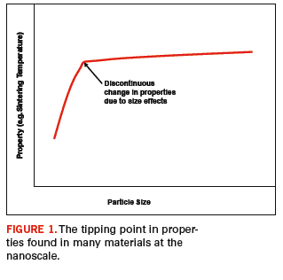
Many materials exhibit a change in properties as they move toward the nanoscale. This is because of the increase in the relative proportion of higher energy surface atoms. This change can be exhibited as a change in reactivity (e.g., sinterability or electromagnetic properties) driven by band gap changes that cause dramatic changes of electronic properties, or optical properties such as color and transparency. Where these changes occur – the tipping point – is a function of the individual element or compound and its environment, and normally occurs below 100 nm (Figure 1).

Solder materials containing nano-sized metals exploit the high surface area and high surface energy (think of it as stored energy) of nano-sized particles to lower the apparent melting point below the conventional melting point. Thus the melting points of tin, silver and copper, the ingredients of most popular Pb-free solders, all can be depressed below 200°C, well below the eutectic melting point of 217°C.7
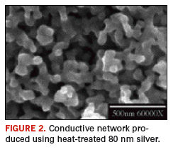
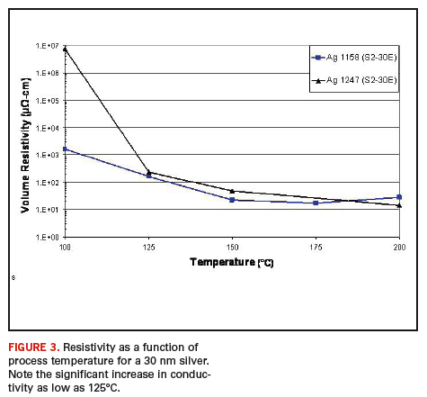
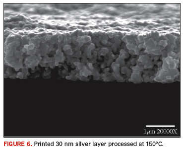
Silver exhibits a dramatic increase in sinterability at temperatures below 200°C. Nano-silver powders can be produced in essentially monodisperse form using a “bottom-up” approach, in which nuclei grow under a protective polymer coat that permits metal atoms to accumulate, while acting as a charge director to keep the embryo crystals separated. The crystals are permitted to grow until the desired particle size is achieved; then the reaction is stopped and the crystals suspended in an appropriate vehicle or dried. The polymer coating, which can be made hydrophilic or hydrophobic, aids re-dispersion and prevents spontaneous sintering of the dried silver particles. Pure nano-metals such as silver can be deposited by a range of printing techniques with a thermally removable binder. Even at 80 nm, significant densification and conductivity development is seen above 125°C (Figures 2 and 3). These show promise for die attach, conductor printing and electrical connections.


The iNEMI Nano-Solder Project is working to put these materials into a printable solder paste. The project team is characterizing the metals and working to develop a proof of concept demonstration, using a model similar to the SnAgCu system developed for Pb-free solders (inemi.org/cms/projects/ba/Pb-free_nano-solder.html).
Nano-solders could potentially be available within the next three years. A method has been developed to synthesize lead-free solders such as Sn-3.5Ag-xCu (x=0.2, 0.5, 1.0) by chemical reduction methods.8 Sinterable silver systems are currently available from such companies as Cabot, Cima NanoTech and NanoDynamics.
Enhanced adhesives. Nanomaterials can enhance mechanical properties of adhesives (even a 0.1% addition of multi-wall carbon nanotubes can raise the flexural strength of an unfilled epoxy by 30%), as well as the electrical properties because of the large number of potential contact or tunneling events when nano-sized particles are present. A reduction of 10x in particle size (for example, from 1 µm to 100 nm) with the same weight content yields a 10 x 10 x 10 (1000-fold) increase in the number of particles present.
Several iNEMI members are participating in a University of Binghamton SPIR project (Strategic Partnership for Industrial Resurgence, http://watson.binghamton.edu/level2/industry.html#SPIR) to quantify effects of nanoparticles – metal and carbon-based – in resin-based systems in order to get a consistent dataset to characterize performance. Information from this project will be published.
Nano-attach technologies. Hook-and-loop fasteners (e.g., Velcro) used the ideas generated by plant burrs to create a new fastening paradigm. An extension would be to use carbon nanotubes, as suggested by researchers at Michigan State University in 2003.9 Simulation of entangled carbon nanotubes demonstrated nanotubes made in curved shapes could be used to develop very high-strength room temperature interconnects.
Another innovative application of nanotechnology is bio-mimetic nano-attach. Textured dry adhesives, based on the gecko foot approach (bio-inspired) where nano-sized hairs attach to surface roughness using van der Waals forces, have been the subject of a great deal of research.10,11 Bio-inspired materials systems using carbon nanotubes or polymer nano-filaments have been demonstrated at a number of research locations with strengths far higher than those that comfortably attach a gecko to a ceiling!
The iNEMI Nano-Attach research project is identifying and attempting to demonstrate these types of nano-adhesion techniques that have the potential to replace traditional solder or conductive adhesive assembly processes currently employed in electronics manufacturing.
Implementation Challenges
Percolation and particles. The addition of fine particles to improve polymer system conductivity has been well documented in the literature. However, duplicating the performance in real-life systems tends to be much more complex. Nano-product implementation can only be achieved if the following factors are addressed:
Protective coating. Virtually all nano-metals need a protective coating that permits dispersion in liquids and prevents oxidation or self-sintering. Uncoated silver will sinter to itself at room temperature, and uncoated copper will quickly turn black. Uncoated aluminum and many other metals are pyrophoric. Coatings may be applied in vapor phase by precipitation or chemical reaction.
Agglomeration. Nanomaterials have high surface energy and tend to stick to each other. Because the number of particles per unit volume is high, the inter-particle distance is lowered as the particle size decreases for a given content. At the sub 5 µm level, many colloids agglomerate at concentrations of only 3 to 5%.
Dispersion. Nanoparticles supplied as dry powders are notoriously difficult to disperse in viscous liquids. The tendency now is to supply them as dispersions in compatible liquids or polymer master batches.
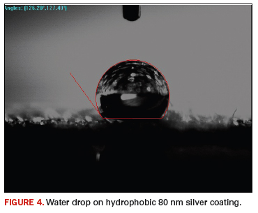
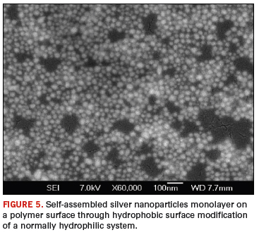
Segregation. By varying the hydrophobic/hydrophilic nature of the surface coating, it is possible to encourage the material to disperse in a similar medium or to preferentially congregate on a second phase or at the surface (Figures 4 and 5).


Reactivity. Reaction with catalysts, fillers or other constituents must be controlled; nanoparticles, by their nature, are reactive.
Sinterable systems. Many of the same issues of surface reactivity apply to sinterable systems (e.g., ink-jettable silver). Surface control is key to controlling reactivity, but the same compromises apply as in adhesives; particles have to be disagglomerated, remain in suspension and achieve a practical concentration and shelf life. The issue is compounded by the fact that many printing systems need relatively low viscosities (tens of centipoises – between the viscosity of water and milk) and many of the inorganic fillers to disperse have high specific gravity compared with the organic pigments we use in many applications. Silver, for instance, has a specific gravity of >11 (much greater than that of organic materials).

Nano-solder. One of the main issues in nano-solder production is the use of tin. It is a very reactive metal and readily oxidizes. (Most of the dross forming on SnPb solder is actually tin oxide.) It is, however, possible to produce tin particles in a reducing environment. Manufacturing oxide-free tin particles, integration of metal particles with flux, and electronics assembly are the focus of the iNEMI Nano-Solder Project. This work is enhanced by a project funded by the National Science Foundation at Purdue University and MetaMateria Partners that is exploring the mechanism of nano-solder consolidation.12 The electron microscopy facility at the Purdue University Birck Nanotechnology Center is carrying out in-situ characterization of the melting behavior of tin and tin alloy nanoparticles. This analysis will be crucial for understanding the melting behavior of nanoparticles intended for use in a solder, and will allow the behavior of individual particles to be correlated with the behavior of a solder paste. This type of fundamental understanding of particle and paste behavior will be necessary for understanding and resolving the challenges related to developing a useable nano-solder.
Nanotube “dry” adhesives. Several challenges include producing the material in the correct form, verifying the theoretical strength and conductivity parameters, designing device interconnects and verifying processability and reliability – and doing it all economically. Nevertheless, this is a game-changing route to assembly that could have real benefits for electronics assemblers.
Conclusion
Nanotechnology provides many useful tools to enhance the properties and processing of electronic materials. The enhanced materials and processes will have to prove their reliability and economic value to compete, but the sheer volume of opportunities and potential solutions suggests we’ll be seeing a lot more nanomaterials in our industry. PCD&F
Ed.: This article is excerpted from a paper in the proceedings of the 2007 SMTA Pan Pacific Microelectronics Symposium and is printed with permission.
References
1. A. Rae and A. Skipor, “Nanotechnology and Room Temperature Assembly,” SMTA: Emerging Technologies Summit, Sept. 25, 2006.
2. C. R. M. Wronski, “The Size Dependence of the Melting Point of Small Particles of Tin,” Brit J. Appl. Phys., vol. 18, 1967.
3. Ph. Buffat and J. P. Borel, “Size Effect on the Melting Temperature of Gold Particles,” Physical Review A, vol. 13, no. 6, June 1976.
4. S. L. Lai, J. Y. Guo, V. Petrova, G. Ramanath, L. H. Allen, “Size-Dependent Meeting Properties of Small Tin Particles: Nanocalorimetric Measurements,” Physical Review Letters, vol. 77, no. 1, July 1996.
5. Leslie H. Allen, “Nanocalorimetry Studies of Materials: Melting Point Depression and Magic Nanostructures,” NNUN Abstracts 2002/Materials, Physics, Process & Characterization, 2002, p. 40.
6. M. Zhang, et al, “Size Dependent Melting Point Depression of Nanostructures: Nanocalorimetric Measurements,” Physical Review B, vol. 62, no. 15, October 2000.
7. Kevin Grossklaus, Melting and Coalescence Behavior of Tin Nanoparticles for Use in Low Temperature Solder Applications, Purdue University, master’s thesis, August 2007.
8. Lin-yin Hsiao and Jengong Duh, “Synthesis and Characterization of Lead free Solders with Sn-3.5Ag-xCu (x=0.2,0.5,1.0) Alloy Nanoparticles by the Chemical Reduction Method,” J. of the Electrochemical Society, 152, (9), 2005.
9. Savas Berber, Young-Kyun Kwon and David Tamanek, “Bonding and Energy Dissipation in a Nanohook Assembly,” Physical Review of Letters, vol. 91, no. 16, October 2003.
10.University of Akron News, “UA Synthetic Gecko Foot-Hairs Leading to Reusable Adhesives,” uakron.edu/news/articles/uamain_1293.php, Aug. 12, 2005.
11. Liehui Ge, Sunny Sethi, Lihie Ci, Pulickel Ajayan and Ali Dhinojwala, “Carbon Nanotube-based Synthetic Gecko Tapes,” Proceedings of the National Academy of Sciences of the United States of America, vol. 104, no. 26, June 26, 2007.
12.Alan Rae, “Nanosolder – What’s Next?” International Conference on Soldering and Reliability, May 16, 2008.
Acknowledgments
The authors gratefully acknowledge the support and contributions of colleagues at NanoDynamics, MetaMateria Partners, Motorola, Purdue University, Delphi, and iNEMI.
Alan Rae, Ph.D., is vice president of innovations for NanoDynamics (nanodynamics.com) and chair of the iNEMI Research Committee; This email address is being protected from spambots. You need JavaScript enabled to view it.. Andrew Skipor, Ph.D., is a distinguished member of the technical staff and distinguished innovator, a nanotechnology leader for Motorola Labs (motorola.com), and chairs of the iNEMI Pb-Free Nano-Solder Project. Marc Chason is an iNEMI consultant and president of Marc Chason and Associates.


