New software tools ease problems associated with power delivery design in large computer systems.
In the late 1990s, the Hewlett-Packard Company entered the marketplace with a large server under the name “Superdome.” This event actually represented a new dimension in the integrated circuit and package design area. The voltage/current pinch and clocking frequencies of the IC’s contained in this new system had increased so dramatically that designers had to design a new tool to model and simulate the power delivery system (PDS) with a higher level of detail.
A voltage/current “pinch” had occured when designers used lower voltages and higher currents at the integrated circuit level in order to pack more gates in the same amount of silicon area without increasing power density. This new generation of IC technology allowed increased complexity while maintaining power per unit area. However, it also created this “pinch” for power delivery, since current increases drawn by the IC, are inverse to the supply voltage, and create larger I*R and L*dI/dt drops in the package, the PCB, and the converter. The “pinch” was tightened by smaller voltage tolerances scaled to the lower supply voltages. Higher currents stress package power planes, solder joints, and PCB power planes, causing excessive heating and reliability problems.
Since that time, there has been the opportunity to redesign several CPU and ASIC packages and learn a great deal in the process. These techniques include a suite of simulations that evaluate the performance of the integrated system from several viewpoints, including methods of interfacing between the IC, the package, and the printed circuit board, either using a fully detailed package model, or with a simplified (IBIS-like) model. The use of simplified models for assemblies, including the packaged IC, can be a time saver, especially if the simplified model is used multiple times at the next level of simulation.
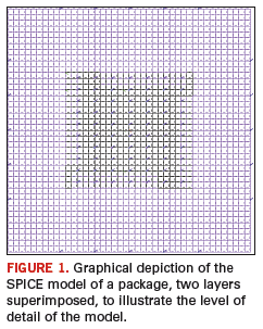
The original tool was actually a large scale SPICE model built in three dimensions. Planar constructions such as IC packages and printed circuit boards can be represented by a stack of two-dimensional square grids, representing the conducting planes, connected vertically with simple circuits representing vias or groups of vias, as shown in Figure 1. Planes and vias are represented as sub circuits including inductances, inter-plane capacitance and resistors as lossy components. Components such as capacitors and resistors are represented with sub circuits, including parasitics of the components and connecting vias.

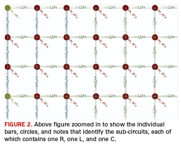
The IC can be represented by a grid of time varying resistors, bypass capacitors, and parasitics, rather like a multi-port IBIS model. The graphical depiction used by the tool is not a conventional schematic, but a map of lines and circles with labels. The model is assembled with the use of a script, which leaves a two-and-one-half dimensional depiction that can be edited manually.
The final graphical model shown in Figure 2 is then processed into a three-dimensional SPICE deck, which is a massive interconnection of sub circuits. The components of the sub circuits must then be evaluated by the user, which is not as daunting a task as it may seem. This SPICE circuit can then be evaluated, yielding voltages, currents, powers, etc. at almost any location within the package. The model is ready for SPICE evaluation in any mode: DC, AC, and Transient simulations can all be done on the same model with minor modifications.

Since the graphical interface does not depend on extraction from a layout tool, it is easily modified for speculative changes and can be used at an early stage in the system design process. On the other hand, most power analysis tools do their models from an extraction of design layout information of an EDA tool. This appears to be a convenience for the power designer, but it delays critical design decisions until late in the design process. We have found that, even though the accuracy of the layout may be less than ideal, the ability to evaluate the performance at an early stage is highly desirable.
A common problem with all PDS analysis tools appears to be the complexity of doing the analysis itself. The device being modeled must be divided into a large number of sub-sections in order to accurately capture the geometric effects of small features. For example, we have found that CPU run times of a week or more can easily happen where a large package is concerned. Where long run time is necessary with a system model, computation time can be speeded up considerably by partitioning the model and substituting simplified units for certain sections of the system model. The simplified model can also enhance communication between levels of the system where the IC design, package design, and system board design are done by different groups. The final section of this paper seeks to explain some of these techniques.
Until recently, the SPICE model approach to package and board analysis was running out of steam because run times were getting too long. In the course of trying to speed up SPICE simulations, we tried comparing different vendors’ SPICE products using the same circuit. We determined that the compute time for at least one new SPICE engine was dramatically improved. For example, we found that a 25,000 node SPICE model could be run in about 20 minutes using a newer SPICE solver where it had taken more than eight days previously. This decrease in processing time is a significant productivity factor.
Power Delivery System Evaluations
The first simulations with the three-dimensional models yielded much more information, and more accurately, than we had ever created before. Much of this accuracy came from the use of a distributed model. With that information in hand, engineers quickly embraced the process, using the new data mainly to improve design accuracy and reduce project risks. Prior to this, the power delivery modeling consisted of a manually calculated one-dimensional network, with consequent errors that often required late corrections based on measurements.
A new process for evaluation of the PDS evolved to include six distinct categories of performance metrics. The important point is that not all of the information produced by the new analysis is useful, so there must be a system for evaluating the data. Some of these categories are more important than others, and my purpose is to explain the importance of each one. Briefly, the six categories are:
DC Voltage Drop. This can be done with a uniform current or detailed map of currents across the die. Actual currents in full activity are used here. The results can determine if excessive voltage drops occur at specific locations on the die. In addition, currents measured at the C4 or bump locations can reveal current density issues or locations exceeding current specifications. In the PC board context, excessive voltage drops and localized heating of planes and vias are important issues. The information can also be used to locate sense points for voltage regulation.
AC Impedance looking into the PDS. From the IC perspective, the package PDS has an equivalent impedance vs. frequency. IC parasitics and bypass need to be included to simulate the response of the merged system. The IC model is a grid of current sources, which add up to 1 amp, all phases at zero. These sweeps can be useful primarily to observe those components or features causing PDS resonances. Beyond that, the model can be used to optimize the frequency response of the PDS by damping out or moving resonances to provide a flatter Z(f). This is easily done by trial and error, by changing bypass cap values and locations. The results of this action can be seen graphically in the transient simulations shown. The die circuit will usually be divided into several blocks, with different current loads, so the single impedance value may not be precise enough for a large IC, and the distributed model would be required. In addition, there may be several power domains that would need to be evaluated individually.
Transient Step Current. This test requires some knowledge of the steady-state operating points of the IC, including leakage and active currents. Generally, the die will be at a low current state if it is idle from a processing standpoint, and jump to a high current draw when called up to full activity. This will produce a “dip” in voltage followed by an overshoot and ringing. This is the most fundamental characteristic of the IC current, and it can reveal problems with inadequate die, package bypassing or PDS resonances. Determining the level of activity or the rise time of the current steps on other vendor’s parts can be difficult to obtain.
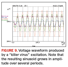
Killer Virus Time Domain Simulation. This is an extension of the transient step current simulation. It is possible, though not likely, that the operation of the die could be directed to cycle from high to low and back at a frequency corresponding to a resonance of the PDS. In this case, the die cyclical voltage could increase in amplitude over several cycles and kill the operation of the die. In simulation testing, this is still considered to be the worst possible stress of the PDS.
Transient Active Current. Once the die design has progressed enough to determine the high frequency switching current drawn by the circuit blocks, these currents can be simulated in the PDS model. The IBIS-like load models are driven separately, or in blocks to fill the grid of die connections. This could also be done in AC mode, but IC designers generally find the time domain graphs more useful. For example, transient current events on the die can occur at the clock frequency, which is usually many hundreds of megahertz and may cause the supply voltage to drop below spec. These transients are usually well above the useful frequency range of the package bypass design. Faced with this, the IC designers can take actions to move timing events to reduce current spikes, or increase die bypass capacitance. Also, this simulation yields a great deal of information at the package/PC board interface which can be used to generate specifications and/or simplified models for PC board designers.
Leakage of High Frequency Noise. When generated at the die level into the PC board power domain, this is a difficult problem to simulate. This could contribute to EMI problems and/or create power related interactions that could limit performance, especially where a large number of IC’s are used in close proximity. Usually, the same model for the package can be used, but the simulation needs to be modified slightly to measure the effects in question.
DC Voltage Drop
This is the most fundamental criterion for the operation of the circuitry on a system board. As simple as it may seem, it should not be taken lightly. The problem can be as simple or as complex as the package or board layout. The voltage/current pinch can happen at any point in the system, and if the designer does not have a good two- or three-dimensional simulation capability, significant errors or omissions can be hidden from view. Voltages in the printed circuit board can usually be probed to find excessive drops. This information is particularly useful in determining the proper copper thickness to use for the power and ground planes, or if additional planes are needed in the board stack up. Currents can be measured in planes and vias to look for places where overheating may occur. This can be a serious problem, particularly under parts with very small pitch and high current densities. In the past, most boards were designed without 2-D simulations However, the changing industry is putting a “pinch” on costs and time to market as well, so the lab that has the better tool set for board design will have the advantage of fewer board turnarounds.
Errors in the package are much harder to fix, since prototype turnaround times are much longer for packages, and costs are higher. The package designer must have accurate knowledge of the DC current drawn by the IC, including the distribution map for a larger die. A three-dimensional model of the package power circuit may be essential to finding overheated bonds or vias and localized voltage drops as well as heating of the planes of the package.
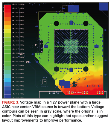
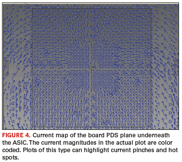
Figure 3 illustrates a plot of supply voltages on a certain power plane within a PC board. The actual plot is in color, which allows voltage drop are subject to be more easily seen. There are no problems in this design, but it illustrates that the current distribution and voltage drop is subject to the shapes of the planes, the placement of sources and loads, and even upon the presence of via keep-outs and thermal relief patterns, which all increase the effective resistance of the planes. Currents can also be displayed as in Figure 4, and hot spots and current pinch areas can usually be found. Computer displays will take advantage of colors to display magnitudes.


There are a number of problems associated with delivering power reliably within a large computer system. Many smaller system manufacturers have not had to deal with these issues on a large scale, but advances in the technology are likely to make these problems much more commonplace. While there are many new software tools designed to deal with these technical hurdles, there is still some confusion surrounding how they are to be used, and how to correlate simulation data through the system hierarchy. In Part 2 of this article, we will propose an approach, including basic, essential, and advanced methods of measuring performance of the PDS, explore methods for linking the simulations of different levels of the PDS, while at the same time simplifying and expediting the task.
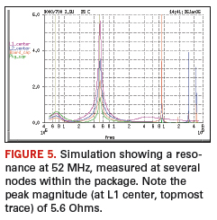
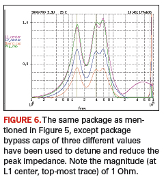
AC impedance is a very useful metric from the PDS perspective. It is generally obtained by placing a current source or array of current sources at the die interface in the package and then measuring the AC voltage magnitude as the frequency of the sources is swept across a large range. Dividing the voltage by the current gives an equivalent impedance, Z(f). This impedance will typically display one or more resonances, caused by the inductances and bypass capacitances in the system. During current transients, this can cause ringing of the supply voltage, and the possibility of exceeding the low or high limits of voltage specifications. Recently, a lot of attention has been focused on reduction of this resonance behavior, including usage of dissipative bypass capacitors and multiple sizing of capacitors on the package and board. Figure 5 illustrates such a resonance in an early version of a package design. The Z(f) plot reveals the resonance at a number of locations within the package, which has bypass capacitors mounted at 20 locations surrounding the die. Figure 6 shows the same package, except the arrangement of several different capacitances serves to break up the resonance and reduce its peak impact.


Despite the usefulness of the Z(f) plot, it leaves many questions unanswered. In Figure 6, the resonance peak is reduced five times, but the magnitude of the impedance in other frequency regions increased. Depending on the spectrum of the current draw by the die, this could be a worse situation than before. Even if we can obtain a frequency plot of the total voltage response produced by the die, there may be variations across the face of the IC. The AC response of the PDS provides very valuable information, but more is needed. We must have a transient simulation, and we may need information on the voltage drop at critical locations across the die.
Transient Step Current
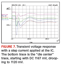
This technique is a favorite of power system designers everywhere. It basically provides information that is equivalent or at least similar to the AC analysis. The Fourier transform of the step response could be used to create the frequency sweep and vice versa. The step response can be applied more directly to the power draw behavior of a real IC or a system of packaged ICs and can be more meaningful to engineers that deal with transient simulations on a daily basis. It is also easier to specify as a performance metric of a given part. For example, Figure 7 shows the response of the package model to a step in total current (80% to 100% in 3 nS for one of the power domains. The data show the initial DC voltage before the step, followed by a steep drop immediately after the step; then a ringing at two different frequencies and an exponential damping characteristic.

Ringing frequencies can be estimated from the plot by measuring periods. The ringing frequency usually agrees with the package resonant frequency and its Q factor observed in the AC sweep discussed in the previous section. This analysis includes actual currents that are expected at the IC and provides instantaneous voltage information. When the first versions of the IC model are available, two states of the circuit are extracted: 1) an idle current with no traffic, and 2) a max traffic current where the die is working at full capacity. Presumably, the circuit will make this transition quickly and quite frequently. The initial droop (such as the droop to 1120 mV in Figure 7) reveals the limitation of the on-die capacitance to respond to current changes. Between the die and the first package bypass capacitance is an inductance that will limit the dI/dt, causing the voltage droop that you see. The only cures for this droop are to reduce the package inductance, increase the on-die capacitance or reduce the dI/dt drawn by the IC. Since the PDS is a linear system, in this simulation, the same amount of overshoot will occur when the load is reduced from full load to 80% of load.
The damping effect on the ringing is brought about by several effects, including the ESR (equivalent series resistance) of the bypass capacitors, the resistance of the package materials and the finite resistance of the IC circuitry itself. The real circuit is not a current source but rather a resistor that varies its resistance to change the current that it draws. This type of simulation should use a programmed resistor rather than a current source to draw the measured currents. In this way, the damping effect of the circuit itself is included. In some instances, the magnitude or the slew rate of the transient may not be known, and several variations of this simulation may need to be performed.
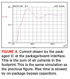
The current step simulation is specific enough to develop specifications for the component parts of a power delivery system and how they function together. The voltage droop in Figure 7 is one example where the synergy of the IC and package designs is tested. Extending this idea further, the current crossing the package/board interface is easily compiled. Manufacturers use the step current specification in their part descriptions quite frequently, since it is valuable information for the system designer. The board power designer can place a current source in his model at the location of the part and proceed with the analysis. Figure 8 shows the level 2 package current corresponding to the simulation in Figure 7. The height of the step and the dI/dt of the waveform can be measured easily in the simulation. This information is important in determining the amount and values of the on-board bypass capacitors and the bandwidth required from the VRM. It should also be noted that the waveform exhibits the limitations of this specification: the ringing of the waveform is a consequence of the passive Z(f) of the device and use of a current source ignores that effect.

Simulations based upon the current step are usually quite adequate if they indicate that there are comfortable margins for error. If the system simulation is indicating marginal or unacceptable noise levels, or some parts of the IC are drawing much higher currents, it may be necessary to opt for more elaborate simulations, not only to try new design approaches but to also establish confidence that the problem has been fixed. The use of a more descriptive time domain current source is the next step.
Killer Virus Transient Simulation
Barring full knowledge of the component part for a complete transient active current simulation, this technique uses step current information and knowledge of the resonant frequencies of the PDS to produce a “speculative worst-case” situation for the simulation. If the component part can pass from lowest average current to highest average current at random times, it is possible that it will do so repeatedly at a repetition rate equal to the period of a PDS resonance. In this case, the voltage across the device would build-up over several cycles of such excitation, reaching a maximum peak-to-peak voltage determined by the current step magnitude and the “Q” of the system resonance. The name “killer virus” comes from the concept that an “assassin” software virus could be designed to excite this mode, and possibly kill the operation of a computer system. Figure 9 illustrates the PDS oscillation that results from such a “killer” waveform.

The killer virus simulation addresses a very limited type of excitation and should be run as many times as necessary to target each resonance of the system. It may easily be the most severe stress that the system would ever encounter; however, it could lead to over-design of the PDS. The actual load may not produce waveforms that fall into this category, so designing to the worst-case situation may not be necessary. For instance, if the worst-case approach does not incur a great deal of cost increase, then the extra safety factor is worth it. But if the cost increase is very large, the choice lies between performing a more accurate analysis or taking a risk that could lead to project delays or product field problems. The transient active current simulation can reveal more inclusive waveform characteristics that would otherwise be missed by this technique and others.
Transient Active Current
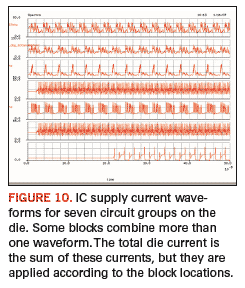
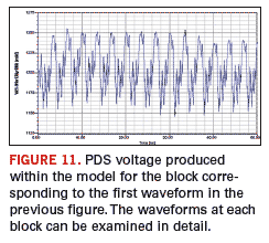
Although the current step and killer virus methods go a long way toward characterizing the package and system response, there is no assurance that the worst-case simulation is represented or that the PDS is optimized to the circuit. It is usually the only approach early on in the design project, since more precise information is not available. The hardest part of the transient active simulation can be obtaining the proper current draw information. We have had the luxury of being in contact with IC designers who can run IC simulations with ideal power supplies and measure the current drawn from those supplies. The designers usually give us data in large piecewise-linear listings, representing the current drawn by “blocks” of circuits. In return, they want to know what the PDS voltage looks like for those blocks under this current draw. Figure 10 illustrates such an ensemble of circuit supply currents.

The IC is divided into several irregular shaped blocks, meaning that the model of the IC power load must be constructed with a number of load models arranged in a pattern that accurately represents the map of the die. In a similar fashion, the current map of a packaged part on a PCB may need to be divided into a grid of models to represent the footprint of the package. When the model is simulated, the geometrical effects of the current paths are automatically evaluated, as are the interactions with adjacent blocks or packages. In one instance, a particularly current hungry block was found to be “borrowing” charge from capacitance in an adjacent block by way of the package planes. This kind of information is very difficult to obtain by any other means.
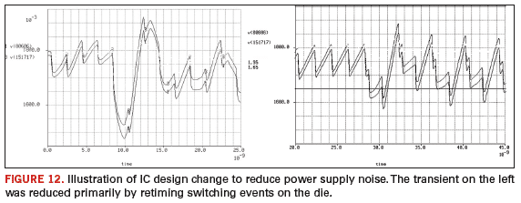
Given that the current draw information is available in detail and that the detailed 3-D model is in place, a close examination of all aspects of the voltages in the system is possible. Certain events on the IC can cause high current transients that were unforeseen in the initial analysis. An example of such a transient is shown in Figure 12. The analysis indicated that an expensive modification to the package design would be needed to handle this current spike. However, when presented with this data, the IC circuit designers came up with a plan to move the timing of the blocks to reduce the total dI/dt of the event.


The ability to do this type of simulation depends on the cooperative effort between the designers on both sides of the interface in question. As devices and systems stretch performance capabilities, design practices must change accordingly. Today, very few vendors are willing or even capable of providing the information required for transient active current analysis. In the case, where only the step current spec is available, the evaluation of the PDS may end at that point. This brings up a difficult decision point for the system designer – whether the step current analysis indicates sufficient margin, all errors considered – or whether to put more pressure on the part supplier for information. In the long term, it may be necessary to improve the power sink and power distribution specification with some new standards. Our research has yielded at least one technique for expediting the compliance process for PDS design.
Backward Leakage of High-Frequency Noise
Increasing high-frequency noise in ICs can produce problems for inter-die communication and generate radio frequency interference (RFI). The higher switching speed of new generation ICs is a fact of life, but it puts a strain on the co-design of the entire PDS. The highest frequency components can only be bypassed by on-die capacitance, which puts a heavy load on the IC power designer. The package and board bypass capacitors typically have too much ESL to effectively short out the gigahertz and higher frequencies. Using proper design practices, the inductance of package planes and vias can be used to advantage to block high frequencies. The use of embedded passives has also been employed for this purpose. Electronic band gap structures have been employed for this purpose as well, but more esoteric techniques such as plane shaping and slotting have also been effective in reducing resonances, power noise and EMI in PCB designs. Vendors of ICs need to be able to specify the level of high-frequency noise that will feedback to the board PDS. Better yet, they should strive to provide models that end users can use in their system simulations.
Reaching for Advanced Design Techniques
The six evaluation techniques just discussed can all be performed to some extent with the most basic IC, package and board models. Designers have probably tried to use some form of them in past projects. Computer systems today are changing in complexity, power density, voltage/current pinch, clocking frequency and cost competition, requiring more comprehensive analysis techniques. Power system design automation products are becoming available from many vendors, so engineers now have tools to attack these problems. Despite the growing selection of these tools, there seems to be a lack of understanding of how to use them, along with a corresponding lack of standards for power system coordinated design. For example, we have been in the process of integrating certain tools into our design space. Tool 1 did not do DC analysis or allow speculative design before a board layout was available. Tool 2 would only do one port for the IC model. Tool 3 delivered S-parameter models that were non-passive. We found ourselves telling the vendors how to design their tools to get the results we needed. During this process, it became painfully obvious that the tool vendors thought we wanted colorful computer displays of currents and voltages. However, we were not prepared to link their models to other models, such as connecting a package to a PCB. We have developed a technique for joining the modeling processes for die to package to PCB that has enabled more accurate and timely simulations. In most analyses, the IC, package and board models are quite complex in their own right, and combining all of this complexity into a single model would use a great deal of computer time and produce a huge amount of data that would be discarded anyway. Enter the simplified model, the first cousin of the IBIS model, adapted to power delivery analysis.
The simplified model can be applied as a proxy IC power net or a package-level substitute. The model can substitute for any module; for instance, we have also applied the model as a proxy DIMM card. The principle is to replace a complex model with a simplified substitute at an obvious interface location. For instance, the DIMM card interface was its edge connector. There will be some loss of accuracy, but the designer must weigh it against the advantage of time to completion.
The process of generating a simplified model begins with a detailed model of the device in question. Where a system is to be modeled, the process begins at the smallest unit. This would be the IC die in most cases, but it could be the VRM, or both, where the system board is the root unit.
Using the IC as an example, it would be necessary for the IC block designer to assemble simulations for his block using the nominal supply voltage as an ideal source and capturing the current draw of each distinct circuit in the operating mode of choice. There will be large numbers of these circuits within the block, so multiplication and addition of the current waveforms is necessary to represent the total current draw of the block. The IC will be represented within the package model as a grid of nodes (or ports) located each in a specific block. For instance, block A may have 27 ports within its boundaries. The block current from the simulation of block A is divided by 27, and applied equally to each of the 27 ports. The same is done for all blocks until the complete map of the die circuit is populated. This mesh of loads is connected to the detailed model of the package, which must be designed to accept these port connections properly.
The currents above may be just waveform driven current sources, but they will have non-zero admittance at each location. The most significant part of that admittance is the on-die bypass capacitance (including resistance). It has been found that the resistance of the die circuits themselves can act as a damping factor. This can be simulated by creating a waveform-driven conductance in place of the current source. The variable conductor draws its current from the voltage source at the board side of the package.
The simulation can proceed; knowing that the low/high voltage is produced by the dynamic voltage variation in the PDS, we can say that the PDS is in spec if the dynamic Vdd voltage remains within the specifications. Usually this approach is satisfactory, although there are other tolerances in the system that may derate the supply Vdd. The evaluation could be carried one step further by rerunning the exact IC simulation, except with the dynamic Vdd captured in the PDS simulation. This last step represents a second-order correction but is usually hidden by errors such as silicon PVT variations and manufacturing tolerances.
This complex model can be used as is, within a higher-level PCB or larger PDS model. We used the above-mentioned SPICE technique to model entire boards, all the way back to the DC-to-DC converters. The PCB can be modeled with a coarser grid. Although this method reduces the node count, it can still produce a model with so many nodes that it can have convergence and run-time problems. It is usually desirable to simplify the package model to dramatically reduce the node count, and conveniently hide the inner workings of the package and IC design.
We have successfully employed several approaches to this “simplified” model. Let us examine the technique applied to a package model simplified for use within a system-board model. The simplified model development calls for voltage and current information looking into the package from the PDS side. The PCB-level analysis requires a minimum of two items discussed as follows.
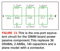
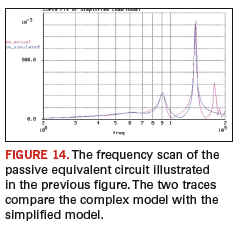
With a passive load, the board PDS will see a passive impedance Z(f) looking into the package from the Level 2 interconnect. This can be measured in the original detailed model by setting the IC loads to a nominal resistance, then driving a grid of current sources at the Level 2 plane of connection. The analysis is an AC sweep, and total current is 1 A. There are obviously a number of voltages available in a multi-port model, so a single representative node must be selected to create a single impedance model. One could create a matrix of impedances, but it would be a lot of work for little benefit. A multi-port S-parameter model could be created, but it would defeat the purpose of simplification. Rather, a single port S-parameter model or a discrete RLC network usually works quite well. The impedance characteristic is simple enough to match very precisely with a network of 10 to 20 elements. Figures 13 and 14 illustrate the creation of such a model.


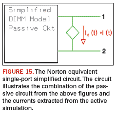
A parallel current source – the current source element of the Norton equivalent circuit – is developed by a second simulation of the package, this time with a voltage source in place at the Level 2 connect. This model element must draw current from the system board as if it were the ASIC package itself, operating in one of many possible modes (see above). This current is the result of the current drawn by the IC, which is modified considerably by the intervening package. The waveform of the current drawn from the Vdd source is captured during the simulation. This now becomes the driving waveform for the system board simulation. The parallel-connected passive load and waveform driven current source now represent the active ASIC part.
This simplified model can then be used in place of the ASIC when evaluating a board-level power delivery system. The similarity to an IBIS model is no mistake. This model is reduced to its minimum complexity and does not reveal the internal details of the ASIC power delivery workings. The model can also be divided into n pieces with 1/n current and admittance, where it is desirable to create a current draw over the grid area equivalent to that of the ASIC. Although the creation of the model is fairly involved, the IBIS-like features would allow a vendor to distribute the model to customers without risk of IP compromise, offering several operating conditions, in a form that is simple to use in SPICE simulations. For example, the model of the DIMM card mentioned earlier was used 32 times in a SPEED 2000 model of a large memory board. The memory board model ran in 20 minutes, which not only verified the operation of the system board, but also allowed multiple iterations on bypassing, power plane variations and power sources. Without the simplified models, the system model would have included 32-DIMM cards, 64 AMBs, and 1152 DRAMs. The simplified passive model is shown in Figure 13, while the comparison of the impedances of the complex and simplified models are shown in Figure 14. Figure 15 illustrates the complete circuit, and it also shows insertion of an added current representing the DC component.

We have also researched two-port simplified package models that provide both Level 1 and Level 2 access points. This model is actually not difficult to synthesize, given a set of procedures. This model can enable studies where the effect of package bypass or VRM options on the component ICs can be measured. Looking forward, the set of procedures to create such a model could be automated to the extent of generating and placing them into the next level of the system model.
Conclusion
This paper presents a review of our experience dealing with the problems delivering power reliably within a large computer system. Many smaller system manufacturers do not have to deal with these problems, at least not on a large scale, but advances in technology threaten to make them much more commonplace. While many new software tools have been designed to deal with these problems, there is still a good deal of confusion surrounding how they are to be used and how to correlate simulation data through the system hierarchy. Facing some of these large-system problems at an earlier time, we were obliged to develop our own tools and techniques to deliver products successfully. At this time, we are seeing a lot of industry-wide concern that power delivery problems are getting out of hand, but from our viewpoint, this need not be the case. A host of powerful tools are coming of age, but we feel that the knowledge gap at this time is the lack of a unified approach to the analysis of the PDS. We have attempted to propose such an approach, including basic, essential and advanced methods of measuring performance of the PDS. We have also proposed methods for linking the simulations of different levels of the PDS, at the same time simplifying and expediting the task. These methods suggest a framework for advanced PDS modeling, similar to the IBIS standard that has been generally accepted for I/O simulations. PCD&F
Dave Quint is a master engineer at HP working on IC fabrication, package design, signal integrity and power delivery system integrity and can be reached at This email address is being protected from spambots. You need JavaScript enabled to view it.. Charles Keen is an analog engineer for HP and can be reached at This email address is being protected from spambots. You need JavaScript enabled to view it..


