WLPs may be the answer to the widening gap between device cost and packaging cost.
The packaging industry enjoyed significant growth between 2004 and
2006, based on increased demand for semiconductor and electronic
products overall. However, capacity expansion to address this growth
has been conservative, resulting in some constraints in supply and
higher prices. As a result, many integrated device manufacturers (IDMs)
have expanded internal operations during this cycle (in parallel with
increasing outsourcing) to balance the cost and risk of capital
investments.
There
has also been rapid emergence of new package technologies driving the
need for increased R&D. Furthermore, higher complexity SIP, stack
package, wafer-level packages and Pb-free packages require greater
R&D coordination between the semiconductor and system-level
packaging industries.
The 2007 iNEMI Roadmap
highlights several critical semiconductor packaging R&D areas that
– if not effectively addressed – will limit future success. This
article highlights some market forces driving semiconductor packaging
research worldwide, and summarizes the critical research areas.
Market Trends
Over the past two years, worldwide semiconductor packaging unit
volumes have been growing at a high rate, driven by a strong overall
semiconductor growth cycle. Many older leadframe-based factories have
returned to high utilization rates. There has also been significant
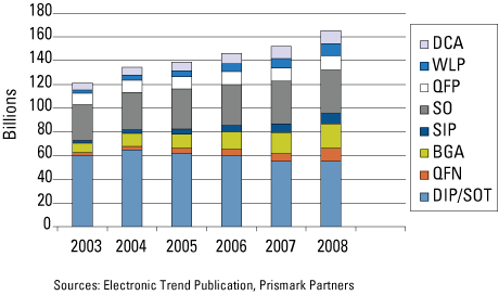
expansion in capacity for newer FPBGA, CSP, SIP, WLP and flip
chip-based packaging (Figure 1). Projections for
expansion indicate newer technologies will continue to grow at a high
rate, while investments in standard leadframe technology will decline.
|

FIGURE 1. Worldwide semiconductor package volume.
|
The primary factors for higher growth rates in newer packaging
technologies are the reduced size, improved performance and lower cost
of these technologies. The higher growth rates have, in turn, shifted
R&D focus to BGA, CSP, WLP and SIP technologies.
In
parallel with the shift, the packaging industry is consolidating
through acquisition of IDM facilities by subcontractors as IDMs exit
non-differentiated packaging; assembly subcontractor mergers; and EMS
companies’ entry into packaging services to expand their product and
service base. In addition, many companies are using technology
development partnerships and manufacturing joint ventures to leverage
R&D resources by sharing costs and reducing capital investment
risk. While this type of research was historically conducted through
open consortia, it has become more common to form private alliances
among companies that tightly protect intellectual property and provide
competitive advantage. As the industry matures, many of these
consolidation activities are expected to continue.
Critical Research Needs
There
are several areas where additional R&D is needed. Substrate
technology, for example, continues to be a key target area with
specific requirements, including improved interconnect density,
reliability and reduced cost. New materials are also required to
address reliability, performance and cost challenges. Thin wafer
packaging and related stacked die have become high priorities since the
2004 Roadmap.
Assembly equipment, in general, is
not keeping pace with needed productivity improvements, and new
processing approaches are needed to shift the cost structure. There is
also a need to improve design simulation and perform chip and package
co-design for very high-performance systems. Integrated standards for
reliability testing and product qualification are required to help
bridge gaps between semiconductor and system standards.
To
focus the industry on research that will yield the highest payback, the
iNEMI Roadmap team identified the critical areas across the industry.
Many of these research needs (Table 1 [PDF format])
cut across multiple package technologies, so they address a large
portion of the market. A few key examples are discussed below.
Low K copper interconnect. To improve device performance,
the industry has transitioned to copper interconnect with low K
dielectrics. The low K/Cu transition has created the need for research
into new copper wirebonding processes, and wafer probe techniques that
enable direct contact to copper metal structures. Low K materials also
have created a problem with packaging because of the lower strength of
these materials. Lower force bonding and development of low-stress
die-to-package interconnect are needed to reduce the risk of die damage
during assembly and temperature cycling. There is also a need for
additional reliability research to further understand the interactions
between new die structures and lead-free solder interconnections, and
to develop package designs that will help reduce this risk.
Wafer-level
packages. WLPs, which provide complete protection and an interconnect
structure for direct mount of the die to a system board, are being
developed to reduce size and cost. For this technology to reach its
full potential, manufacturers must develop high-reliability
WLP-to-substrate connections that can support area array pitches below
100 µm. If this type package is to be broadly adopted, it will be
necessary to reduce cost by eliminating expensive underfill processes.
Thin
packaging and die stacking. These technologies have been developed to
increase density, particularly in memory applications. However, both
types require wafer thinning advancements. Today, the thinning of
300-mm wafers below 100 µm leads to significantly increased breakage
during handling. The reliability of these thin die, which use lower
strength low K dielectric materials, is also a concern. Industry trends
will drive the need to thin below 50 µm in some configurations. At this
thickness, many die structures are dominated by the properties of the
die metal and dielectric.
Interconnect density. As
semiconductor device features continue to shrink, the gap between
die-level interconnect density and package interconnect density will
continue to increase. Today, semiconductor interconnection features are
in production at 65 nm, while area array off-chip interconnect is
limited to 200-µm pitch I/O features, which are difficult to route with
state of-the-art substrate technologies. The need for a radical
improvement in chip-to-package I/O density and substrate density is
clear, and the solutions will most likely be based on completely new
approaches, rather than the evolution of existing technologies. Related
to this need are requirements for new materials, including organics
that can provide improved TCE match to silicon, lower moisture
absorption, higher temperature compatibility and reduced cost.
Reduced
packaging costs. In many market applications, semiconductor device cost
has continued to drop at a faster rate than packaging cost. The 2007
iNEMI Roadmap projects a 5% per year drop in the cost per I/O for
packaging, while many market sectors are driving the need for a 15% per
year reduction in product cost. New technology approaches are the key
to reducing package cost, particularly given recent increases in base
material cost. WLP, which can eliminate many package assembly process
steps, may be one technology that can help drive this cost reduction.
Reliability.
Development of new test methods and reliability test standards is a
pervasive theme through almost all new areas of package development.
New materials and structures are much more complex and push reliability
boundaries of many applications. To address this, iNEMI has proposed an
industry-wide program of collaborative research to develop test methods
that will help identify and characterize failure mechanisms. The second
phase of this program has also been proposed to develop test standards
based on identified failure mechanisms. (For more information, contact
Bob Pfahl at iNEMI; This email address is being protected from spambots. You need JavaScript enabled to view it..)
SiP
and 3-D packaging. Two areas of research that have evolved quickly
during the last two years are SiP and 3-D packaging. SiP technology is
primarily being driven by the mobile phone industry, which requires the
integration of many device types into small form factor packages. SIP
technology trends are summarized in Table 2 [PDF format].
3-D packaging is a longer term development focus that has
the potential to shift the entire industry structure and technology
base. There are many different competing approaches to 3-D, but they
have some common elements, especially in terms of development needs.
One critical element is the formation of high-aspect-ratio via
structures that can enable interconnect of nanometer scale structures
in three dimensions. Approaches to cool these extremely dense
structures need to be developed.
Development Process
The
packaging roadmap was developed by a group of industry experts
representing IDMs, assembly contractors, equipment suppliers, materials
suppliers and research groups across the industry. This group also
supports development of the ITRS Packaging Roadmap. As a result, the
tables on critical research needs and packaging technology are used in
both roadmaps. The iNEMI Roadmap, however, provides additional
information on market trends and the business conditions that impact
the pace and scope of worldwide packaging research and development.
Work
will soon begin on the 2009 Roadmap. Anyone interested in participating
can contact Chuck Richardson, iNEMI director of roadmapping; This email address is being protected from spambots. You need JavaScript enabled to view it.. PCD&F
Joe Adam is vice president of operations for Wispry (wispry.com). He chaired the packaging technical working group of the 2007 iNEMI Roadmap.


