A comparison of energy, water and chemical use for two common processes.
“We will make decisions based on sustainability, Lenora.” I heard the words clearly. I understood the tone in his voice and the impact it would mean for the industry moving forward. Interestingly, it was not the only time I would hear that same statement within a few weeks.
Over the past years, the term “sustainability” had been something of a buzzword. We see it in our everyday lives and, honestly, I don’t always understand it. We have eliminated plastic bags at many stores, but now I’m collecting reusable bags by the handful. What are customers supposed to do with all these bags? Many end up in the trash, especially when they are being handed out similarly to a disposable product. Is it better that they are not plastic, or is it just as bad because we are creating the same level of waste?
This makes my head hurt. I need to see things in a basic form to make sense of it and determine if it is an improvement – or not.
Now my customers have started asking about sustainability comparisons for chemical processes in printed circuit board manufacture. My thought is to start with the basics: Energy usage. Water usage. Chemical consumption. These are things I can track and show without worrying about the type of energy used at the fabricator, or the price of energy regionally, let alone daily fluctuations. I start with tangible concepts.
When we look at chemical processing or what we call wet chemistry, a few inputs immediately come to mind for energy usage. The solutions must be heated to achieve performance, solution flow or movement is critical in delivering material to the board’s surface and within the holes, and circuit boards need to be transported through the process. All aspects use energy. This is in the form of heaters, pumps to create and deliver solution, and motors that drive the boards through the process equipment.
The next resource is water usage. Rinse quality is critical to the success of the product. A consistent flow of fresh water to remove residual chemicals from the board’s surface and holes is essential. Poor rinsing can result in quality and performance issues later in manufacture or final build.
Last is chemical consumption. This is how much material is used to create a successful product. It will vary for each process type and for each step within that process. To ensure a good product, continuous replenishment of fresh chemicals is necessary to keep everything in balance. A well-balanced formulation results in controlled plating rates or etching rates and ensures brightness or proper grain structure, and overall balance delivers the desired outcome. Chemicals leave the bath through absorption onto the circuit board, drag out of solution from the plating tank or chemical breakdown.
It is important to look at all aspects of a process when delivering the information to the customer. Depending on the region, some areas may be of greater concern than others. When the PCB technology teams at end-users began making these requests, I expected their areas of concern could be different from those of a circuit board fabricator. Yes, all parties are conscious of power, water and chemical usage, but to requalify a process for a small improvement can be a major strain on an end-user. I have been in the industry long enough to know that a minimal improvement is not perceived to be worth the time, money or resources to make a change. It is best to show a process change that will have a “double-digit improvement over the incumbent.”
Internally, we have begun calculating kilowatt-hour (KWh) consumption for segments of our business, so I understand that certain areas have a greater energy footprint than others. I decided to start with one of the more complex processes in PCB fabrication, one that is highly resource-intensive. It is one that every board experiences: primary metallization. The most common is electroless copper plating. I hope to shed some light on specific details that we as a chemical supplier focus on, details that might not be clear to end-users or others in the supply chain.
Primary metallization, sometimes termed “making holes conductive,” takes a dielectric substrate and deposits a conductive layer for subsequent electrolytic copper plating. It is necessary to make the dielectric conductive and further build copper pathways that carry electric current. As stated, the most common process used is electroless copper plating in a vertical application. After the resin and copper are properly cleaned and prepared, parts are processed through a palladium solution, a step called activation. Palladium is a catalyst for copper deposition and adsorbs to the surface of the dielectric material. This gives the copper an active site to bond.
The electroless copper cycle is a multistep process with complex chemical baths. It contains different metals to deliver the palladium, reduce it and then plate copper. All are required to achieve uniform coverage. The copper plating bath itself uses reducing agents and chelators. It is an operation that requires close attention to all process parameters for success. Though there are complexities to the system, it accounts for 80% of the market share and has been a viable process since the 1950s. It is used for all market segments and board design types.
An alternative, simplified process is called direct metallization. Direct metallization uses a carbon or graphite seed layer to make the holes conductive prior to electrolytic copper plating. A conditioning step creates a uniform charge over the surface. In the coating bath, the carbon material electrostatically coats the entire board. Unwanted carbon on the copper foil or innerlayers is etched away prior to electrolytic copper plating. It is called direct metallization because clean copper innerlayers entering the electrolytic plating bath result in a direct copper-to-copper bond. (By contrast, in an electroless copper process, the palladium and thin copper layer stand between the innerlayers and the electrolytic plating.)
Direct metallization uses three chemical steps that are very stable in nature. It does not require metals or chelating agents in the formulation, which makes for easier control of the chemical constituents. It has been on the market for over 30 years but is considered the newer technology. It is heavily used in flexible circuitry and low-loss materials due to its process capabilities. It is the primary metallization of choice for the handheld and substrate package markets due to its ease and short cycle times when manufacturing multilayer high-density designs with microvias.
Resource Reduction
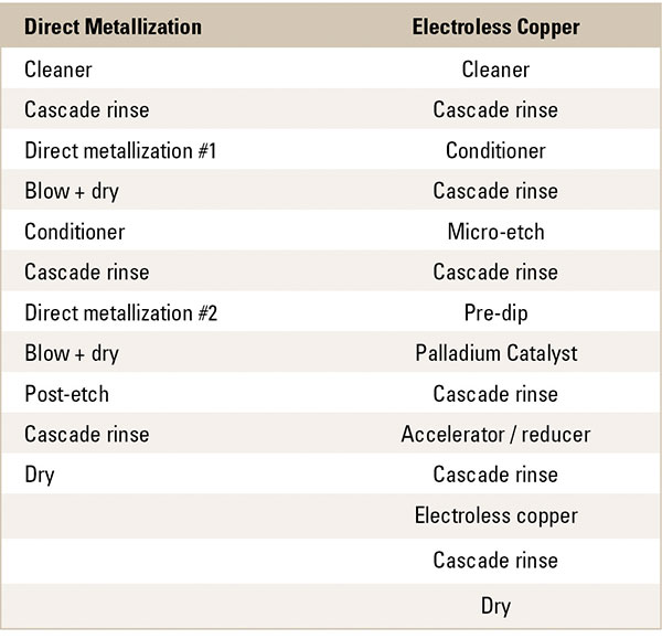
The reduction in resources for direct metallization becomes clear when you compare the two processes. TABLE 1 shows the chemical and rinse steps required for each. Direct metallization can be run in a single pass mode, but to deliver the worst-case figures I have chosen a double-pass process (known in MacDermid Alpha as Blackhole Double Pass). To normalize the vertical and horizontal applications, consumption of two production lines manufacturing 20,000m2 per month are compared.
Table 1. Metallization Chemical and Rinse Steps

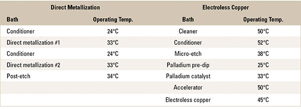
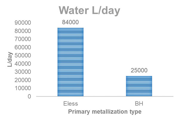
Electroless copper has seven chemical steps and six rinse steps. Direct metallization has three chemical steps, one of which is used twice, and three rinse steps. For the electroless process, the chemical baths on average run at higher temperatures than they do for direct metallization (TABLE 2). Immediately, a reduction in water usage is realized. FIGURE 1 compares water usage for one day: 25,000 liters for direct metallization and 84,000 liters for electroless. It is a 70% reduction in water used per day.
Table 2. Comparison of Metallization Processing Temperatures


Figure 1. A double-pass direct metallization process uses 70% less water per day than electroless copper, based on a line producing 20,000m2 per month.
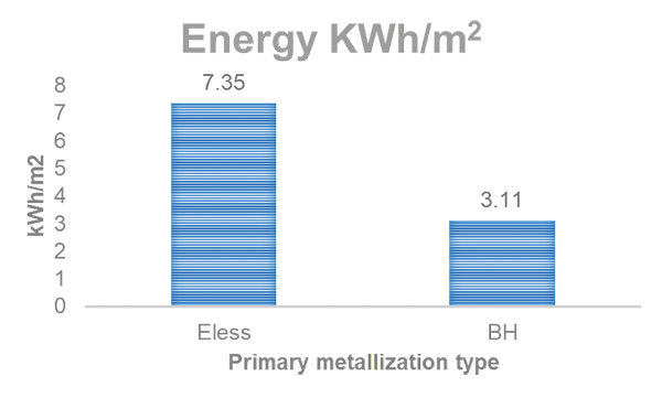
Energy usage can be viewed per month or per square meter. Assuming again both lines are producing 20,000m2 in a month, the electroless copper line uses 147,000KWh and direct metallization uses 62,250KWh. Dividing by 20,000 to realize the energy per square meter comes to 7.35KWh and 3.11KWh, respectively, or a 58% reduction in power (FIGURE 2).

Figure 2. Direct metallization also uses about 58% less energy than electroless copper.
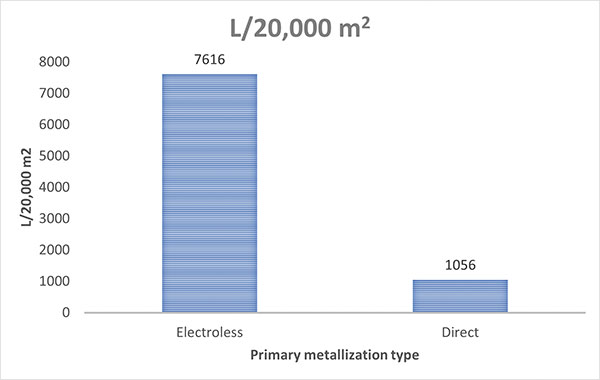
The final resource of chemical usage is a bit more complicated. A chemical solution can go out of balance in multiple ways. This is due to metals plating out of solution, materials being dragged from the plating tank on the board surface or in holes and chemical breakdown. The main challenge plaguing the electroless copper plating bath is the Cannizzaro reaction.1 This reaction happens immediately upon mixing. In our case, the caustic and formaldehyde form sodium formate and methanol. The chemical byproducts are likely not the main concern of this audience, but what should be understood is that growth in these materials puts the bath out of balance. It is necessary to bail out or remove a certain volume of the bath regularly to decrease the growth of side products and replenish with fresh chemistry. This, in combination with multiple metals being deposited on the board, causes high chemical consumption over the course of each bath life. Comparing chemical consumption of electroless copper to direct metallization shows the greatest difference in resource usage. The usage per month of the 20,000m2 processes are 7616L and 1056L, respectively (FIGURE 3). The direct metallization process reduces chemical usage by 86%.

Figure 3. Likewise, this direct metallization process reduces chemical usage by 86%.
Reliability Effects
The utility savings are evident when comparing the two processes. Of course, the next question is regarding reliability of the process and resultant product. Carbon and graphite direct metallization are always processed horizontally, which delivers the same solution to all surfaces without the isolation zones created when running a vertical process in magazine form. Racking vertically is most common for electroless copper. A horizontal process is available but with extensive floor space required and some limitations when switching between substrate types.
Another substantial difference between the two is the effervesce created during processing. Electroless copper creates bubbles that can get captured in holes or in microvias. This will hinder coverage and subsequent copper plating. This will not happen in direct metallization; no bubbling occurs in the coating bath.
Direct metallization utilizes stable chemicals that enable a wide operating window and no dramatic changes are needed when moving from one substrate material to another for the coating process. Direct metallization has served many markets successfully for over 30 years and a host of reliability data are available. It is a proven solution for sustainability. •
References
1. Cheryl A. Deckert, Ph.D., “Electroless Copper Plating – A Review: Part I,” Plating & Surface Finishing, February 1995; https://www.nmfrc.org/pdf/p0295g.pdf.
Lenora Clark is director of Autonomous Driving and Safety at MacDermid Alpha Electronics Solutions (macdermidalpha.com); This email address is being protected from spambots. You need JavaScript enabled to view it..


