A design can look good on paper, but has it been vetted for manufacturing?
Printed circuit board assembly: What comes to mind when you hear, read, or think that term? What does or should this mean to a printed circuit board designer or a printed circuit engineer? Is it an afterthought within the overall process of designing and manufacturing your product in the rush to get your product to market the fastest while trying to minimize your cost?
For me, what pops into my head is design for manufacturability or excellence (DfM or DfX), which includes fabrication and assembly – but let’s not forget producibility as well.
Let’s first understand what is meant by design for manufacturing. It is a design technique for accounting for all the constraints of the assortment of parts that constitute the final product after assembly. DfM focuses on minimizing the complexities involved in manufacturing operations as well as reducing the overall part production cost.
Now, let’s understand what is meant by producibility. It is the relative ease of manufacturing a product or system. Quality in design focuses on concurrent development of the total system using capable manufacturing processes, leading to a producible, testable, sustainable and affordable product that meets defined requirements.
I strongly believe that assembly (manufacturing/production) and producibility need to be accounted for from the earliest conceptual stages in the design process. Collaboration and integration among all key stakeholders of the product to be designed are essential in the quest for success in printed circuit engineering.
From building component libraries to finalizing layouts, assembly and producibility must always be considered important factors to address. It’s one thing to get a technical query (TQ) from a fabricator regarding the PCB, but it’s significantly different when issues present themselves downstream in assembly or production.
Here’s why. At the PCB fabrication stage, there is still potential (time) to make a change to a design to ease manufacturing (fabrication) before it is set in stone. Once a PCB is fabricated, it’s in a physical state that cannot be changed without serious ramifications. At the assembly or production stage, the PCB is already locked in. At this point in the overall process, it is what it is! It’s too late and too far downstream to address “design” changes to the PCBA at hand. The potential for rework, workarounds, or worse, revisions of a PCBA become extremely costly.
Throughout my career as a printed circuit engineer, I have engaged with other PCB designers, design engineers and manufacturing engineers (fabrication and assembly) at industry trade shows like IPC Apex and, especially, PCB West. From the newest generation of PCB designers and engineers to seasoned veterans, it amazes me to hear how the accountability of assembly or producibility details, which must be addressed early in the process to ensure successful PCB assembly, are still often overlooked or fall much lower in the list of design priorities when it comes to printed circuit engineering.
I often hear horror stories from both sides, from design engineering teams to manufacturing and producibility engineers. For instance, the inability to place connectors on an assembly because the outer shell of the connector was not accounted for in the library during part creation, and now there is component-to-component interference.
Another example is edge connectors placed too close to each other at the edge of a PCB. The land patterns together fit perfectly in the design at layout but are physically impossible for human interface once at assembly.
Then there are component solderability issues with land grid arrays (LGAs) or bottom-termination components (BTCs), and component toe and heel fillet issues, component courtyard issues, and design for test (DfT) issues.
Don’t get me started on designs that are almost impossible to rework, or designs that require extensive customization to assemble from the very beginning. This includes designs with lots of manual component placement in combination with automated component placement. Depending on the requirements, the product may see multiple thermal cycles throughout the assembly process before it leaves manufacturing and ships out. Now, because of the potential of excessive thermal cycles, latent product failures are potential nightmares. A few other horror stories I’ll mention include mixing lead-free and lead (Pb) components on the same assembly, as well as those conformal coating nightmares. I can go on and on with horror stories when it comes to assembly and production.
I can usually point out one factor at the core of these horror stories. Assembly or producibility were not accounted for, or were a vague thought, during the design process of a product. The design was completed without that key assembly and producibility stakeholder involvement upfront. The product was designed and figuratively thrown over the wall to manufacturing, with the highest expectations from the project team that there will be no issues manufacturing or assembling their product. With a wave of hands like a magician, presto: Manufacturing will resolve any issues and return with an assembled product.
This is not what happens, of course. Personally, I find that engineering approach inadequate and disrespectful to the manufacturing assembly and producibility professions when it comes to printed circuit engineering. We have encapsulated the three competing perspectives today’s circuit engineer must meet for success. FIGURE 1 visualizes this design triangle.
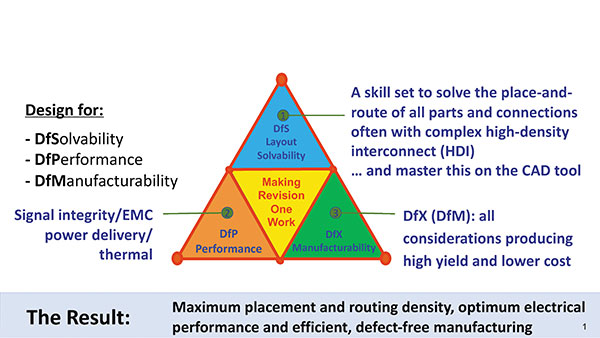
Figure 1. The design triangle. Today’s circuit engineer must meet three competing perspectives for success.
In engineering, we often hear the phrase, “The devil is in the details.” When it comes to PCB assembly and producibility, many details need to be accounted for. More specifically, they need to be addressed upstream in the process. These details, when not considered or incorporated early in the design process, can potentially become your worst nightmare downstream in manufacturing (production). Assembly and producibility issues often lead to extensive rework, schedule delays, and project budget overruns. In the worst cases, it may be catastrophic, especially if components cannot be assembled to the PCB, or if assembly takes an enormous and extensive effort. That’s why it is very important to understand the depth of the concept of DfA and producibility, and why these key factors are so important when it comes to successful PCBA manufacturing. It’s also important to have the manufacturing/production feedback loop in place and maintained with engineering to ensure continued multidiscipline and multidomain collaboration for success from design to manufacturing.
Collaboration between design and manufacturing and how those two disciplines exchange data are important as well. It should be bidirectional. By doing this, we enable lessons learned from manufacturing to be fed back to design. That bidirectional loop (read: data exchange) influences the design and ensures minimal risk at fabrication and assembly. To do this, we utilize intelligent data formats such as ODB++ and IPC-2581. These types of data formats enable detailed communication of design intent from engineering to manufacturing. The value we gain is an optimized, integrated collaboration that contains all the information needed for manufacturing while minimizing errors during the data exchange. And, it provides a continuous feedback loop of lessons learned from manufacturing assembly back to design engineering.
Success starts from the beginning by bringing the assembly and producibility stakeholders to the design table, along with all other vital stakeholders of the PCB design, to ensure a greater potential for success downstream. Upfront collaboration and breaking down the silos between disciplines and domains is the key to downstream success. Today’s EDA tools can create digital threads, or digital twins, that can reduce the costs of trial-and-error and respins.
As stated, success in printed circuit assembly starts early in the process. Manufacturing and assembly fluency, which include producibility, requires understanding industry specifications. Most printed circuit industry specifications are developed by IPC. The IPC standards are created to aid and guide development and offer a common language for printed circuit engineering and manufacturing. Many IPC specifications tie design to assembly; see FIGURE 2 for a list of the IPC standards related to the PCB process.
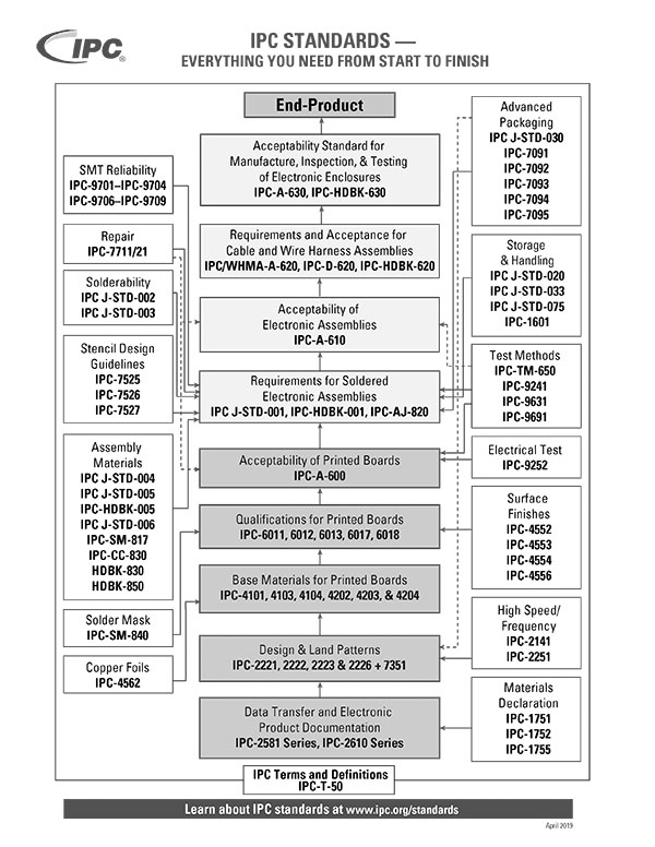
Figure 2. The IPC standards tree, showing the list of specifications from design to assembly.
IPC also produced a free resource called IPC Checklist for Producing Rigid Printed Board Assemblies. I highly recommend this 28-page document to anyone involved with printed circuit engineering and manufacturing. A copy, along with a few other key documents, is available at ipc.org/ipc-standards-related-resources.
When it comes to printed circuit assembly in today’s environment, the devil is in the details, and when it comes to assembly and producibility, there are a lot of details to account for. Make sure all key stakeholders, including manufacturing and producibility, are brought to the table early in the process. Customer requirements, the required performance class and producibility level, and what we are designing and building are extremely important to know and fully understand. As stated in IPC Standards: What Every Manufacturer Should Know, “Electronics are at the heart of millions of products, from aerospace and defense, to automotive, information technology, telecom, manufacturing, retail, healthcare, and more. Our lives depend on electronics in everything we do.” •
Stephen Chavez, MIT, CID+, CPCD, is a senior product marketing manager with Siemens. He has three decades’ experience as a printed circuit engineer, and is chairman of the Printed Circuit Engineering Association (pcea.net); This email address is being protected from spambots. You need JavaScript enabled to view it..


