Dimensional acceptability is incumbent on proper use of IPC-2615 and ANSI/ASME Y14.5.
Two points to be aware of regarding printed circuit board (PCB) dimensional drawings are 1) many, if not most, contain a note saying the drawing is to be interpreted in accordance with ANSI/ASME Y14.5, Geometric Dimensioning and Tolerancing, (GD&T) and 2) many, if not most, of the ones containing the note have not been prepared according to Y14.5. In practice, I have ignored such meaningless notes and interpreted the associated drawing in the manner most reasonable to me.
If a printed circuit board drawing is prepared in accordance with ANSI/ASME Y14.5, information needed to read it is in IPC-2615, Printed Board Dimensions and Tolerances. (A better title might be something like “Specifying Printed Board Dimensions and Tolerances in Drawings.”) If a drawing is not prepared in accordance with Y14.5, the way to read it is not defined unambiguously. Below I will present an example of how ambiguity can lead to uncertainty about a PCB’s dimensional acceptability.
Y14.5 permits preparation of drawings of parts much more complex than most PCBs, which are parallelepipeds with cylindrical holes in the majority of instances. IPC-2615 contains descriptions of the GD&T symbols required to define dimensions of a PCB. The symbols required are a relatively small subset of the complete GD&T set.
Rigid Boards – Rectangular
What I refer to as a “rigid board – rectangular” is a rectangular parallelepiped, meaning, it has six sides. Most of the time, but not always as we shall see, it is fine to think of such a board as being a rectangle.
Rigid boards commonly have three mutually perpendicular “datum” planes, which are idealized planes defining the reference frame in which measurements are made. This definition of the reference frame is fundamental to interpretation of a dimensional drawing. The three planes are usually denoted by the symbols A, B, and C inside squares. FIGURE 1 demonstrates the concept of datum planes.
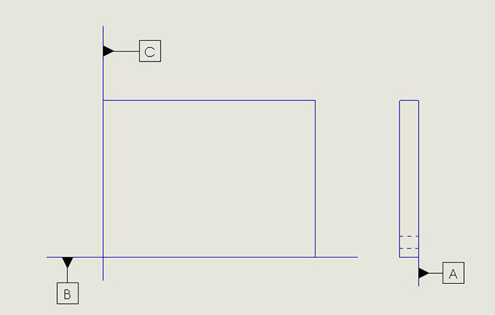
Figure 1. Conceptualization of three datum planes.
Datum planes have a sequence of “precedence” prescribing which of the three is selected first and is thus the “primary” datum, beginning the definition of the measurement reference frame. Subsequently, the secondary and tertiary datum planes are selected. For the moment, let’s say A is the primary datum plane, B the secondary and C the tertiary. FIGURE 9a shows how datum precedence would be defined in a so-called “feature control frame,” the rectangular segmented box containing, from left to right, the letters A, B and C.
By this point, you may be asking, “But PCBs do not have any truly plane surfaces – not the top, bottom, or any of the four other sides. How do we begin to make measurements in reality? Refer to FIGURE 2 for a graphical representation of the following discussion. In the real world, we simulate a primary datum plane such as A, the bottom of the PCB under consideration, by placing the PCB’s bottom surface on a surface plate. The three points of the PCB that make contact with the surface plate define the simulated datum plane A. Secondary datum B is simulated by placing a right-angle reference plane on the surface plate and moving the PCB across the surface plate until the board edge denoted by B contacts the reference plane, which it will at two points. Tertiary datum C is simulated by placing a second right-angle reference plane on the surface plate, perpendicular to the one just used in connection with datum B definition, then moving the PCB across the surface plate and the datum B right-angle reference plane, simultaneously, until the PCB contacts the datum C right-angle reference plane. That contact with datum C takes place at a single point.
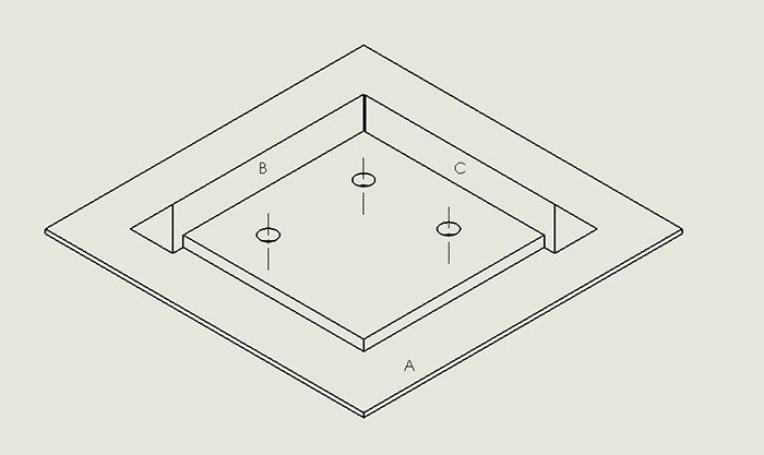
Figure 2. 3-D representation of datum planes.
The precedence of datum planes is important in determining if a rectangular PCB’s dimensions meet the drawing requirements. Consider the simplistic example in Figure 3. Suppose the designer wants a rectangular rigid PCB, with dimensions 1.00 x 10.00, with a tolerance of ±0.05. A “traditional,” non-GD&T drawing of its outline might be as in FIGURE 3a. If the PCB is a parallelogram instead of a rectangle, as shown in the rectangular coordinate system of FIGURE 3b, a measurement of the perpendicular distance between the 1.00 edges would yield 10.00. Likewise, a measurement of the perpendicular distance between the 10.00 edges would yield 1.00. The PCB would apparently meet the drawing requirements. However, it might not fit into the space provided in the application. Now consider a drawing prepared in accordance with Y14.5 (FIGURE 3c). Measurements of the parallelogram according to the datum order of precedence as primary A, secondary B, tertiary C would yield the vertical length as 1.0 and the horizontal length as 10.10, as shown by Figure 3c. Horizontal length does not conform to Figure 3b, and the PCB would be identified as not being able to fit into the provided space.
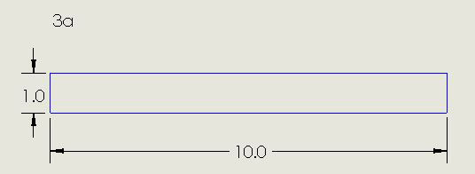
Figure 3a. Conventional non-GD&T drawing of a rectangular PCB outline.
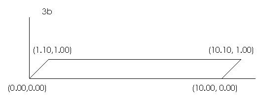
Figure 3b. Conventional non-GD&T drawing of a parallelogram PCB outline.
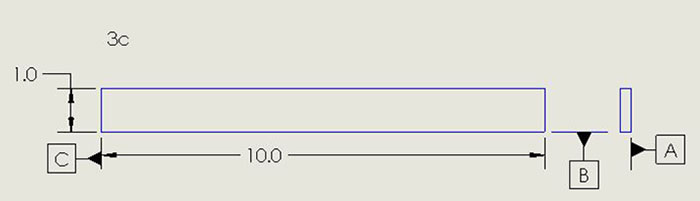
Figure 3c. A drawing prepared in accordance with Y14.5.
FIGURE 4 shows another way often used in PCB drawings for defining the three datum planes. Instead of using a surface and two of the board edges to define the datums, a surface and two holes internal to the PCB perform that function.

Figure 4. A common alternate method for defining the three datum planes employs a surface and two internal holes.
Datum A is, as before, the bottom surface of the PCB.
Datum B is the secondary datum. It is a plane containing the line perpendicular to Datum A and through the center of the hole denoted by B in Figure 4. It defines the vertical orientation of the datum plane B. What defines the orientation of the datum B horizontally? In other words, how is the plane rotated around that line perpendicular to A? Datum C.
Datum C is the tertiary datum. Like datum B, it is a plane perpendicular to A, and it contains the line through the center of the hole denoted by C in Figure 4. It also contains the line identifying datum B – the one through the center of the hole denoted by B. The horizontal x distance from B to C has a tolerance, but the vertical y position of C does not. The y position of C is 0 by definition, as it defines the direction of the line from B.The orientation of datum plane B is thus determined by the requirement that it be perpendicular to datum plane C.
Rigid-Flex Boards
FIGURE 5 shows how datums could be defined for a rigid-flex board with two rigid segments. This approach takes into account possibly large dimensional tolerances in the flexible segment, while providing for tighter tolerancing of the rigid ones.
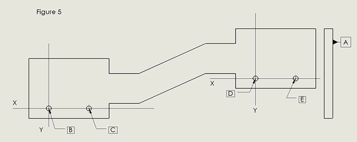
Figure 5. Rigid-flex board datums (two rigid segments).
Datum A is the bottom of the rigid segments, in the same way it was for the rigid boards just seen.
The left-hand segment of the rigid-flex has datums B and C to complete definition of the reference frame for the left-hand rigid segment. These datums effectively construct a frame of reference for the left-hand segment independent of the righthand rigid segment. By analogy with Figure 4 above, the y axis corresponds to the datum plane, which passes through the center of the hole, denoted as datum B. Orientation of the y axis is defined as perpendicular to the x axis, which passes through datums B and C.
In the same way, datums D and E complete definition of the reference frame for the righthand rigid segment.
Circular Boards
Drawings for non-rectangular boards, the only examples of which I have seen are circular, likewise require definition of a reference frame. This includes boards with curved edges. From FIGURE 6a (modified from IPC-2615), you can get some idea of how non-rectangular boards or those with circular shape might be drawn. Datum K is akin to the Datum A seen above and called the bottom of the board. Datum M is the axis through the center of the circle circumscribing the board. Notice the M symbol does not point to the center of the circle directly. Since the pattern of holes exhibits rotational symmetry around Datum M, there is no need for a third datum to indicate the orientation of any pattern of features internal to the board. FIGURE 6b demonstrates this concept. The mutually perpendicular planes intersecting at Datum M could have any orientation with respect to the internal features, although it is most convenient for construction of the drawing to have one of the planes passing through one of those features as shown in Figure 6b. In a moment I will demonstrate the simple way non-symmetric feature patterns are handled.
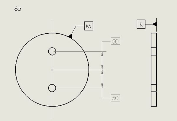
Figure 6a. Drawing for non-rectangular or circular-shaped boards.
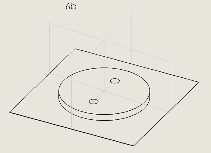
Figure 6b. 3-D rendering of non-rectangular board drawing.
Let me digress briefly and call attention to the boxes around the 50s. A box surrounding a number denotes a BASIC dimension, meaning the dimension has no tolerance. Here, the boxes define “true position,” which is where the centers of the four holes are intended to be in relation to the planes intersecting at M, as described above. Drawings made according to Y14.5 or IPC-2615 routinely specify tolerance for departures from true position, using language like “holes must be within 3 mils of true position.” (More on defining hole locations and how GD&T offers the optimal method is shown in the Hole Location Tolerance section.)
When a circular board has a hole at its ideal center, the axis of the hole may be used as what I referred to above as Datum M, i.e., in lieu of the axis of the circumscribed cylinder.
Circular boards with a non-symmetric dimensional feature pattern, such as a tooling hole or slot, must define three datums, as we have seen for rectangular boards. The approach is analogous to that seen in Figure 4. In Figure 7 (as in Figure 6), K and M are the primary and secondary datum planes. When the non-symmetrically oriented feature pattern is, for instance, a tooling hole (FIGURE 7a), its axis serves to define the tertiary datum. In analogy with Datum C in Figure 4, Datum N defines that tertiary datum plane. (Location of the axis of this hole would be defined by its true position as described above and its location tolerance as in the Hole Location Tolerance section below.) Non-symmetric features would be then specified with respect to these three datum planes.
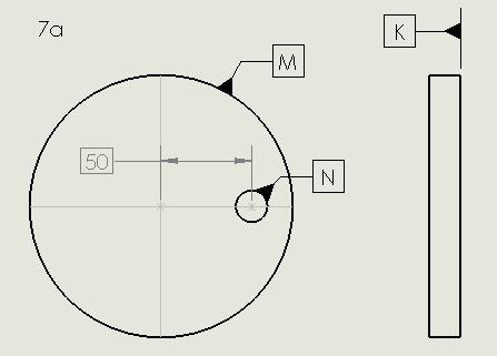
Figure 7a. When a non-symmetrically oriented feature pattern is a tooling hole, its axis serves to define the tertiary datum.
If the non-symmetrically oriented feature is a slot, as in FIGURE 7b, the definition of Datum N in IPC-2615 appears to show some lack of clarity. If the plane of symmetry of the slot, perpendicular to Datum K, contains the Datum M hole axis, that plane would define Datum N as I interpret IPC-2615. However, if by some manufacturing mishap the slot’s plane of symmetry is skewed with respect to Datum M, how does one define Datum N? Expressing this point more precisely, what physical features on the PCB are used to simulate Datum N?
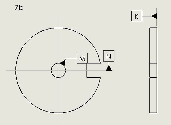
Figure 7b. The definition of Datum N per IPC-2615 for a slot feature is open to interpretation.
Profiles
Figure 8, adapted from Figure 7-2 in IPC-2615, shows how a drawing can require the edges of a nominally rectangular board fit within a region in a manner akin to the way a piece of glass must fit in a window frame, i.e., by how much the board shape can depart from that of a perfect rectangle. FIGURE 8a demonstrates the concept, with 1.0 wide tolerance zone for the PCB profile. Notice the tolerance zone applies from the perspective of looking down on the top of the board AND looking down the long edges, as suggested by the righthand part of Figure 8a, which defines the familiar Datum A. FIGURE 8b exemplifies how a drawing in conformance with Y14.5 or IPC-2615 denotes a profile requirement. Figure 8b has translated the meaning of Figure 8a into a format less concise but easier for the uninitiated to interpret. The semicircle in the leftmost square of the string of three (the feature control frame, to be dealt with in more detail in the next section) indicates a requirement on the board profile. The small circle at the bend of the arrow indicates the profile requirement applies “all around” the board perimeter. If the small circle were absent, the profile requirement would apply only to the edge of the board to which the arrow points.
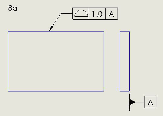
Figure 8a. A drawing can require the edges of a nominally rectangular board fit within a region in a manner akin to the way a piece of glass must fit in a window frame.
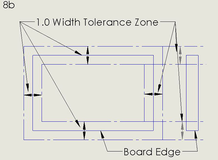
Figure 8b. Another rendering of the profile requirement in Figure 8a.
Incidentally, “leader line” is the jargon for what I referred to above as “arrow.”
Hole Location Tolerance and Feature Control Frames
Notice in Figure 9a the feature control frame – the long, segmented rectangular box. Feature control frames are common on drawings. The one in Figure 9a defines the tolerance of position of the hole, for instance, the center of the hole, to which the line from it points. The ideal location or true position of the hole is specified as 10.0 from datum B and 5.0 from datum C. Those numbers in boxes are basic dimensions, as described above.
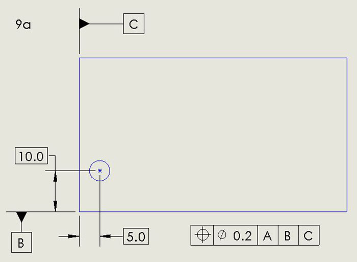
Figure 9a. Here, the feature control frame – the long, segmented rectangular box – defines the tolerance of position of the hole.
The allowable departure from true position is defined in the feature control frame as follows:
- The circle-cross says the feature being defined is a position, in this case the position of the center of the hole.
- The circle with a slash followed by 0.5 says the diameter of the tolerance region is 0.5. (The units of measurement would be in an information block, commonly in the lower right corner of the drawing.)
- A, B, and C boxes, reading from left to right, define the primary datum as A, secondary datum as B, tertiary datum as C.
Let me observe at this point that tolerances on hole position may be defined unrealistically by rectangles in old-fashioned drawings. Y14.5, as in FIGURE 9b, defines departures from true position in terms of a circle, in this case of diameter 2.88. This circle may be thought of as circumscribing an old-fashioned rectangle having length and width of 2.0, for example, representative of a rectangular tolerance of ±1.0. Y14.5 thus provides an additional area in which the hole may be located. The area of the circle within which the hole position may lie is more than 1.57 times as great as the area allowed by the rectangular dimensioning.
Personally, I have had to reject PCBs whose hole locations were outside specified rectangular tolerance limits, but which would have been within tolerance if the locations had been specified by Y14.5.
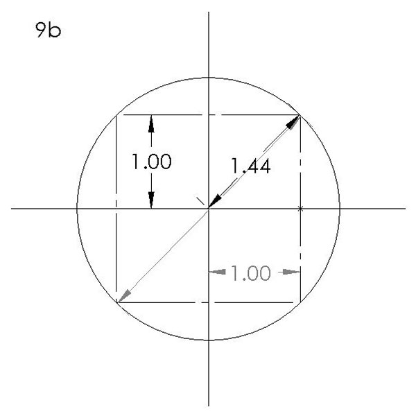
Figure 9b. Departures from true position, as defined by a circle.
Perpendicularity
Ideally, the axis of a hole in a PCB is perpendicular to both external surfaces. Excessive departure from perpendicularity will impact usability of tooling or mounting holes. FIGURE 10a shows an example of the specification of perpendicularity tolerance via a feature control frame. The inverted T symbol, familiar from geometry, indicates perpendicularity is being specified. The circle bisected by the diagonal slash and the following 0.1 defines the tolerance on perpendicularity (FIGURE 10b). A cylinder of diameter 0.1, perpendicular to the bottom surface of the PCB, must circumscribe the axis of the hole.
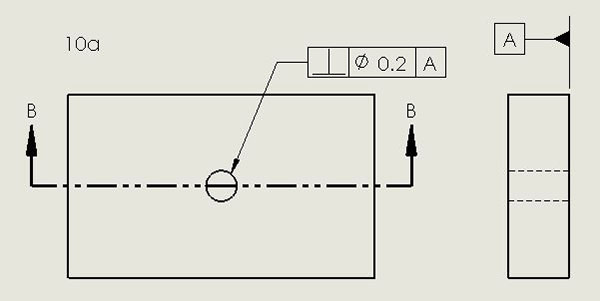
Figure 10a. An example of the specification of perpendicularity tolerance via a feature control frame. The inverted T indicates perpendicularity is being specified.
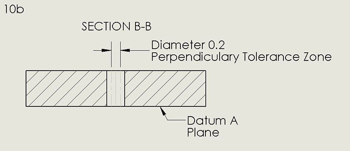
Figure 10b. The diagonal slash and the following 0.1 define the tolerance on perpendicularity.
Summary
Below is a summary of the PCB characteristics IPC-2615 says you will see on PCB drawings in feature control frames. The first four are the most frequently used. In fact, IPC-2615 has no commentary related to the other five. For a detailed explanation, refer to Y14.5.
- Position – location of holes and land patterns.
- Profile – departure from perfect form of board edges.
- Perpendicularity – inclination of the axis of a hole with respect to the board surface.
- Angularity – orientation of one feature with respect to another feature.
- Concentricity – departure from colinearity of axes of two features in a PCB, for example, with a bonded heat sink.
- Flatness – alternative to specification of bow and twist.
- Circularity – departure from perfect cylindrical form of a circular PCB.
- Parallelism – departure of a PCB surface from its perfect form distance with respect to a datum plane.
- Straightness – akin to parallelism, but applicable to a line or region of a surface and not referenced to a datum plane. PCD&F
Acknowledgments
Thank you to Brandon Coates of Touchstone Research for assistance in preparing the figures.
Louis Hart is a retired printed circuit board engineer; This email address is being protected from spambots. You need JavaScript enabled to view it..


