These lead frames are for a wide variety of applications, including semiconductors, glass-to-metal seals and relays; are also used in medical applications such as hearing aids. Base materials include kovar, nickel-iron alloys, copper alloys and pure nickel; can be plated in entirety or selectively. Pb-free materials include silver, nickel, gold or tin, depending on customer conductivity requirements.
These large, high-complexity PCBs are for use in compute-intensive applications such as servers and mainframes for defense, aerospace and commercial applications. EI reportedly can provide high-density, double-sided hybrid PC board assemblies (SMT/PTH/press fit) with an average component count of > 1500, including high-I/O area array modules (CGA, LGA, PBGA) and dense, high-I/O connectors, in sizes as large as 32" x 44".
PCB12 3.0 design software uses a free distribution model. Is said to extend PCB industrial-grade design environment with a high-throughput user interface; fully defined DRC/DfM rules; real-time order quoting, and 'click-to-order' function. Upgrades include integrated schematic and layout, bidirectional schematic/layout synchronization, schematic auto-wiring, auto-placer and auto-router, and real-time DRC 12 layer board support.
The MultiPress S is a microprocessor-controlled bench-top
multilayer lamination press said to be ideal for creating multilayer circuit
boards. Is said to be a tool for rapid PCB prototyping, with a pressing time of
fewer than 90 min. Bonds multilayer circuits of all common rigid and flexible
substrates. Delivers equal pressure on the full press plate area. Nine
heating/pressing/cooling process profiles can be programmed into the system,
with a max. press area of 9" x 12" and temp. up to 482 °F (250 °C);
can bond RF-multilayer substrates.
This high-speed robotic palletizing solution uses multiple
robotic arms. Enables four-way orientation of cases. With full control of
package label positioning, customers reportedly can showcase the same graphics
on all four sides of the pallet, or orient barcodes to streamline scanning
operations.
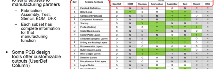
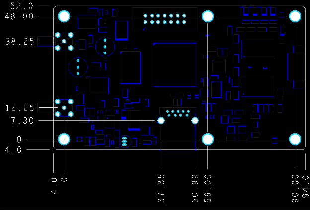
BluePrint for PCBs Version 1.8 creates
documentation that drives PCB fabrication, assembly and inspection. Delivers a
new ODB++ based interface to Altium Designer. Extends the concept of “rolling
releases”; customers are said to receive a continuous stream of improvements.
Includes advanced visibility controls for components, pins, nets, drills, ref
designators, part names and attributes; extended drill support; side view
modifications; CAD style grid support; explode and side view modifications;
usability enhancements, and software corrections.