The core elements make up the not-so-simple foundation of a PCB design project.
Understanding key schematic design fundamentals is of utmost importance when beginning a PCB design project. This foundation of knowledge begins with what a schematic is and its main purpose.
Creating a schematic diagram is a way for an engineer to quickly document the elements of a complex circuit in a way that can be easily read and understood. A properly captured schematic helps the PCB design process by hierarchically organizing the electrical areas of the evolving PCB design.
A complex schematic drawing package, or design database, usually starts with a system-block diagram showing all the parts of the design on the first sheet. A completed schematic should look basic to any viewing stakeholder, such as a field service tech or test engineer. However, stakeholders such as those involved in design and layout leverage the vast amounts of data embedded within the ECAD schematic to complete the design layout.
Standardization. Through the years, engineers have used creative methods to capture schematics. Capture software has very few input requirements and can be used by anyone to make connections between almost anything. For instance, ECAD tools today are so easy to use, even a surfer with no electrical knowledge could create a schematic symbol for a beach hut, a surf shop, a surfboard, and a wave and tie them together with connections to show other surfers what they would be doing throughout the day (FIGURE 1).

Figure 1. Sample schematic for a day in the life of a surfer.
Examining this simple schematic, it is easy to see the surfer is going to leave their hut, go to the surf shop, come out with a surfboard, and head for the ocean to surf a wave. Now, ask three different EEs to draw a schematic depicting a surfer’s day. As you can imagine, each EE will have their own take on what the beach hut looks like: Does it have a back door or a basement; is it solar-powered or off-grid? How an EE would depict a surf shop or surfboard schematic symbol is anyone’s guess. When it comes to depicting a wave, let’s just say EEs can be very knowledgeable about waves observed on an oscilloscope, but schematically depicting a wave viewed from a beach will again yield a wide variety of interpretations, leading to confusion among those trying to decipher these simple schematic drawings.
The electronics industry foresaw this issue years ago and, as a result, organizations formed to standardize the way schematic symbols are depicted. ASME Y14.44-2008 and IEEE 315-1975 define how to reference and annotate components of electronic devices. FIGURE 2 is a short list of reference designators and their matching symbols. A complete list is on the IEEE website at standards.ieee.org/standard/315-1975.html.
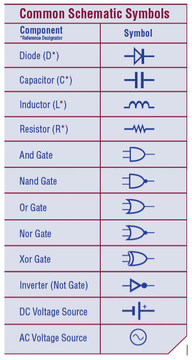
Figure 2. Standard schematic symbols.
Successful schematic capture is basically the process of creating simple schematic symbols that contain simple nodal contacts. These symbols represent simple part configurations that are each documented on a page of the manufacturer’s data sheet.
The goal of capturing the schematic is to define or “capture” as much data as required to be imported into the layout database, so it can be leveraged to create the physical aspects of the design. As mentioned, the schematic is a simplified, symbolic representation of what will materialize as a physical PCB assembly (FIGURE 3).
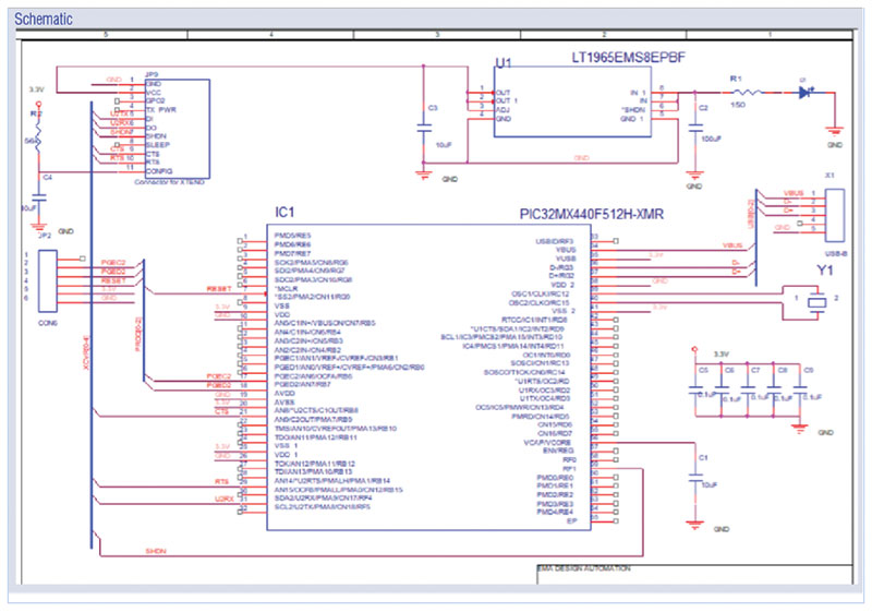
Figure 3. A sample schematic drawing.
Default values and software automation. Many undesirable outcomes can stem from naively using default values and blindly launching software automation. If you were to replicate a simple schematic symbol that contains incomplete or misunderstood data hundreds of times in a schematic, the results would be catastrophic.
So ECAD suppliers have made schematic capture easier, right? Well yes, but it’s not inherently simple. Over the years, to help address complex design issues, the ECAD industry has unintentionally complicated schematic capture by adding vast amounts of complex functionality. It is now the responsibility of the EE to investigate these complexities, and understand them thoroughly, before implementing them. As mentioned, a basic ECAD schematic library symbol represents the connectivity of an electronic part within a circuit on the schematic. However, the explosion of ECAD tool functionality has required electronics designers to take on a much more holistic view of the selected part. Information beyond pin assignment and connectivity can now be embedded into the part symbol. Functionality can be added to the modern schematic symbol to access multiple PCB layout footprints that contain 3-D representations of the part – a recent boon to the quickly emerging mechatronics movement.
As we can see, the simple building blocks of a schematic diagram are no longer simple due to advanced requirements for functionality. They remain the building blocks, so it is more important than ever to confirm every attribute entered is accurate.
Schematic layout best practices. When creating schematic symbols, simplicity is key. There are not many rules regarding the creation of a symbol in a schematic, unless they are predefined in an internal company design specification. For EEs working on a design team, it is essential for a symbol to have some form of consistency.
Symbol creators are free to replicate the part connectivity information in the symbol almost any way they see fit, but for those without preexisting company standards, a couple of basic guidelines will help with consistency:
- For bidirectional discrete parts, consistently orient the symbol within the editor either horizontally, with pin one to the left, or vertically, with pin one at the top.
- For unidirectional part symbols, follow the same guidelines as mentioned for bidirectional, but carefully consider information that may need to be added to the symbol to prevent the part from being installed backward.
Communicating design intent and design tips. Effective communication of design intent is an essential part of the schematic design process. Since it will be used by various stakeholders through the design cycle (review, layout, testing, etc.), schematics need to be easy-to-read and understand. As mentioned, schematic readability is subjective, so keep the end-user in mind and organize it in a way that is anticipated by the reader.
Questions to ask before you begin designing:
- Are special notes or performance requirements expected?
- Do current-carrying capacity or impedance need to be noted?
- Will the schematic be viewed electronically or on paper?
To create an effective schematic layout, follow these tried-and-true tips:
Include as much information as possible. This includes part values, manufacturing information and net names. Have a good library of parts containing all the necessary symbols, footprints and part attributes. This will reduce errors throughout designs and save time.
Determine if the design with be flat or hierarchical. This will also help with the flow of the schematic. A flat design is a single or multi-sheet design with all pages at the same level. A hierarchical design includes one or more modules which can be opened to view the corresponding schematic. These can be used for complex, multi-sheet designs where the circuit is broken down into building blocks and are typical when reusing parts of circuitry, like a power module.
Schematics: Anything but simple. While a completed schematic should look basic to any viewing stakeholder, the information included within is anything but simple. Stakeholders, such as those involved in design and layout, leverage the vast amounts of data embedded within the ECAD schematic to complete the design layout and influence decisions along the way.
Schematic diagrams can range from straightforward to complex, based on the design captured. However, the methodology used to capture the schematic can be kept simple by following industry standards, implementing consistency, common sense, and knowing what to watch out for.
This excerpt of The Hitchhikers Guide to PCB Design was written by EMA Design Automation with special contribution from Theodor Iacob. Download to learn more about PCB design stakeholders and real-world, actionable PCB design tips from industry experts (go.ema-eda.com/pcbguide).


