A job-by-job guide to the engineers behind each new project.
Contrary to what many may believe, designing a printed circuit board is not a one-man job. Communication with many stakeholders is a critical part of the design process and an important responsibility of the EE/PCB designer. With the role of electrical engineers quickly evolving, it is important to note successful PCB design is not done in a vacuum. A PCB design will only materialize successfully by a commitment from the EE to reach out and gather information from the PCB industry stakeholders listed below. Each stakeholder will be contributing their part to manufacturing the design and ensuring its overall success.
The program manager. Before the engineering process of a project begins, the program/project manager (PM) considers all the resources that will be required to complete the project. On a well-run project, the PM will ensure certain EEs are well-informed about important details regarding the PCB. The program manager is not an expert in PCB layout, however, and relies on the designer to query about any missing information in the design requirements at this essential phase. The two must define several important key factors upon which the layout will be based.
When conceptualizing the PCB project, a PM obtains specification for how the PCB is to be used. Performance is a key factor in selection of parts, materials and processes for the design. In the early stages of product definition, a designer must seek to identify a performance class for the PCB from the PM to get the layout pointed in the right direction.
The electronics engineer. Electronics engineers (EEs) are well-versed in circuit theory and the components that make circuits perform. They have spent their career devising creative ways to utilize electrical components in ways that would yield the greatest circuit performance at the lowest cost, while providing for the requirements of many project stakeholders.
Since there is always so much in the way of design definition and specification required, there isn’t much time to “carve traces” (although this is changing). Due to this reality, electronics engineers choose to collaborate on PCB design layouts. Traditionally, EEs can provide PCB designers with either a rough draft or completed schematic diagram. However, the industry is now moving toward a hybrid role where the EE and PCB designer are one.

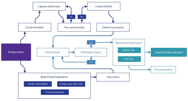
Figure 1. The PCB design-to-manufacturing process.
The mechanical engineer. Mechanical engineers (MEs) work hard for months creating solid model designs for end-product. One of the parts the ME defines is the shape and size of the outline of the PCB, which is a critical component of the product. The ME touches base with EEs throughout the process to make sure the size and shape – the mechanical envelope – of the PCB works with all the electronic components the EE estimates will be required. Once the two stakeholders agree, the ME will freeze the PCB outline in the mechanical layout and begin designing other features around it, while the EE works capture the schematic and may begin the PCB layout using the PCB outline as an important starting point.
The PCB fabrication sales engineer. The PCB fabrication sales engineer (FSE) works for the bare-board PCB supplier. They ensure engineering customers and supplier management personnel questions are answered by the appropriate technical people. If an EE/PCB designer has a question about materials, hole sizing, or how to achieve a certain impedance, the FSE connects the PCB designer with the right technical person to provide the answers. If a purchasing agent wants to order a quantity of PCBs to be delivered to the assembler within five days, they coordinate with their company’s quoting department to establish a cost and timeline.
The assembly manufacturing engineer. The assembly manufacturing engineer (AME) is a master at figuring out how to put a lot of parts together in the fastest way possible – with the highest yield at the lowest cost – by using the best machines and processes. They are responsible for planning, coordinating and performing the manufacturing engineering work for a project.
When working with AMEs it is important for designers to understand that while a PCB layout is designed only once, it can sometimes spawn thousands of PCBs from the bare board supplier. Therefore, it is important designers ask AMEs the important things to consider about assembly before starting a PCB layout.
The test engineer. The test engineer (TE) works with the EE to define the parts of a PCB assembly to be tested. In high-volume production, the ability to test and measure specified features is critical to measuring success. TEs also work with the AME to create automated test beds (or bed-of-nails test fixtures) to audit the success or failures of the AME’s machinery and processes. Both the TE and AME know machines, processes and people are imperfect. Thousands of things can go wrong while manufacturing a PCB assembly. They know good design addresses the requirements for testing and auditing for manufacturing defects. Test engineers appreciate when a PCB design includes small test lands – etched copper “pads” that can be probed with the pins on the test fixture. Probe testers can catch most errors that might be introduced during PCB assembly.
The customer. The customer is the person the end-product is for, internally or externally. They can be the person setting requirements, or the end-user. Keep the customer in mind throughout the design process, so you can make design decisions that will support them. Great engineers approach PCB design from an end-user’s point-of-view.
The PCB Design Process
Just as there are established workflows to guide the progress of a PCB panel through each of its manufacturing process steps, there is an established workflow for the PCB design process. To design a successful PCB, understand these design process steps by building stakeholder relationships. Keep in mind how every decision incorporated into the design will feed the success of the ensuing steps (and people involved) in the manufacturing process.
Contacting stakeholders and manufacturing representatives. There cannot be enough emphasis placed on the value of developing a solid relationship before beginning the design process with the supplier representatives and technical personnel who will be manufacturing the PCB. Establishing a working relationship with EMS providers before starting a design will ensure the designer has a resource for solid manufacturing feedback for the basis of important design decisions.
A great way to be introduced to the design and manufacturing community – its people, machinery, materials, process and software – is to attend one of the many PCB design and manufacturing industry trade shows held throughout the year. Electronics trade shows are renowned for being interactive and informative gatherings where one can eat, sleep and breathe all things PCB. Virtually all stakeholder representatives are always on hand to answer questions and to show their materials, processes and machinery.
Just as established workflows guide the progress of a PCB panel through each of its manufacturing process steps, there is an established workflow for the PCB design process. To design a successful PCB, it is important to understand these design process steps by building stakeholder relationships.
Keep in mind how every decision incorporated into the design will feed the success of the ensuing steps (and people involved) in the manufacturing process.
This excerpt of The Hitchhikers Guide to PCB Design was written by EMA Design Automation with special contribution from Mark Thompson with Prototron Circuits (prototron.com).Download to learn more about PCB design stakeholders and real-world, actionable PCB design tips from industry experts (go.ema-eda.com/pcbguide).


