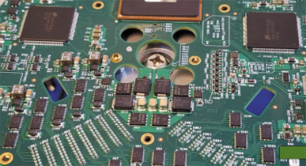
Component manufacturers continue to seek breakthroughs, adding functions and reducing size, while fan-out is left to the designer.
While the printed circuit board is composed of sheets of dielectric and conductor layers, it’s the vias that really bring a circuit to life and keep it going. Permitting signals to pass from one layer to another makes this a 3-D puzzle that can scale to a staggering number of layers.
You don’t have to go back many decades to find a time when we called them printed wiring boards. (Officially, the standards still do.) Components were mounted to what looked like a pegboard: rows of evenly spaced holes where the leads of the part extended through two or more of the holes. You just added wire. As far as routing consistency, every board was a one-off, built up one wire at a time.
Give credit to government agencies for driving PCB technology toward higher reliability. Along the way, the “industrial complex” responded with the following electronics innovations:
- Individual transistors advanced to integrated circuits using dual-inline package technology.
- Axial- and radial-leaded passive through-hole components gave way to surface mount types with and without leads.
- Quad flat packages (QFP) and similar devices came along with a full perimeter of signal pins, plus a ground slug taking the central area inside the single ring of pins.
- Ball grid array (BGA) packages now featured a partial or full field of pins.
Each of these general categories describe a watershed advancement in device packaging as we went from one transistor to billions of them. The PCB industry responded by transitioning to multiple layers of etch, which protected the more vulnerable circuits and permitted higher circuit density.

Figure 1. A typical mix of components found on a board that features through-hole vias.
Component manufacturers continually outdo themselves, adding functions while reducing size. The end game is a “marketing breakthrough,” where the company can compare its chipset to the others and claim to take up the least amount of PCB real estate. While that claim may be technically true, the part where the fan-out is left to the designer is the unspoken cost of chip-scale packaging.
The standard plated through-hole via. The plated through-hole via still has a long runway. On plenty of devices, the pitch of the pins supports through vias in the go-to size of 8-mil drill with 18-mil capture pads on all layers. This is the usual size for Class 2 commercial applications and permits up to 90° of the drilled/plated hole to break out from the 18-mil pad. Thicker boards want larger holes, as the fabricator doesn’t want to deal with plating high aspect ratio holes. The common 0.062" board thickness is in the sweet spot.
(I will continue using mils for drill/pad sizes and metric units for device pitches. The two systems are blended in the real world, where there are CAM operators and SI/PI people who use mils, and they set the rules. Meanwhile, the chipmakers have settled into decreasing the pin pitch from one rounded metric number to another. I could call it 127µm or 5 mils. The point is to be comfortable with the common units of measure.)
Now, where was I?
Class 3 design rules for high reliability. On the high-reliability side, we still use the 8-mil drill but with a 23-mil pad on the outer layer and 21-mil innerlayer. These numbers are intended to ensure a minimum 2-mil annular ring of metal around the hole on every layer. This must account for layer-to-layer registration, along with hole location and size tolerance.
The vias described above are useful for routing DIP and QFP packages, along with the roomy BGA devices where the pin pitch equals or exceeds 0.8mm. Be careful about managing the vias in the thermal pad that makes up the heart of the QFN/QFP package types. You might get away with adding a few regular vias between the paste stencil openings.
When the device is consuming a considerable amount of current, more vias must be placed in the thermal pad. The vias may be filled with a nonconductive material and capped with metal plating so solder cannot migrate down the holes. Last, a conductive fill with little globs of copper mixed with strands of silver in an epoxy base is the plan for drawing out some serious heat.
Case study: Thermally conductive fill. The end of a fiberoptic cable has a transponder that converts light waves from the glass into electrical waves for copper and also generates the light waves going the other direction using a laser. These photo detectors and lasers get very warm as the units strobe along at 10 to 400Gb per second.
In one case, the mechanical engineer thought they had an answer that used a slot in the board and a pedestal in the housing to pass through the board and contact the bottom of the device. The engineer didn’t want to believe the PCB could not have a +/-1-mil thickness tolerance. It was a 1mm board, so the standard tolerance was +/-4 mils. That didn’t help the engineer’s pedestal plan, but it’s always good when the fabricator confirms your statements.
They tried everything: thermal pad, grease and different heat sinks. Only one configuration had a measurable difference: the one where I changed the ground holes in the center pad from 10 mils to 13 and had them filled with the expensive two-step thermal epoxy fill. The measurable difference was it met the spec, and we could ship products to Cisco.
General-purpose PCBs continue to use plated through-hole vias. Plated through-hole vias are sufficient to fan out BGA packages with lower pin-count and generous pin-to-pin spacing of 0.8mm or more. It may be possible to use PTH vias on a 0.65mm-pitch BGA, although it uses a 16-mil capture pad. It is likely you will hear from the fabricator if you go this way, even if the finished hole size is decreased to 6 mils.

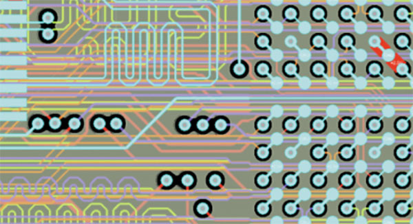
Figure 2. A fan-out scheme for the FPGA shown in Figure 1.
You need to use the 1mm- or 1.27mm-pitch devices to pull off a high-reliability (Class 3) fan-out. The number of layers required grows quickly as each via blocks the routing channel on every layer. We’re lucky if we get two traces between the vias. Necking down traces to fit the geometry may not sit well with those signal integrity folks.
Rounding out the plated through-hole via discussion. Thankfully, some FPGA and ASIC vendors still deal in packages that can be used with a 10- to 12-layer board with through-hole technology. Back-drilling may be required for the thicker boards. Extra thin traces and spaces may be required in especially dense areas to allow the signals to escape from the inner part of the BGA devices.
In cases where the vias are incorporated with a heat-sink pin, plugging and capping prevents solder migration, while vias filled with thermally conductive material can dissipate a lot of energy.

Figure 3. Opening up the solder mask for the vias provides a convenient method of attaching a jumper wire.
A row of large vias can be placed along the edge of a board and cut off right down the middle for what’s called a castellated via. The ground net or even various signals can wrap around the edge or a slot somewhere within the board using castellated vias.
Other than components targeted for mobile applications, many possibilities exist to build a PCB using through-hole technology. Power consumption may be higher while edge rates are lower than their miniaturized counterparts. Some of these more robust parts may only be available in the high-temperature version.
If these things aren’t concerning, then perhaps basic PCB technology can be used for simpler projects in a way that extends the expected lifespan. You have to hope they keep on building those components.
John Burkhert Jr. is a career PCB designer experienced in military, telecom, consumer hardware and, lately, the automotive industry. Originally, he was an RF specialist but is compelled to flip the bit now and then to fill the need for high-speed digital design. He enjoys playing bass and racing bikes when he's not writing about or performing PCB layout. His column is produced by Cadence Design Systems and runs monthly.


