Effects of passive geometry or topography attributes common to PCB layout.
High-speed signal integrity is often influenced to a greater extent by the printed circuit board’s physical parameters than the chosen laminate material. High-speed laminate materials with a low dielectric constant or permittivity, , and dissipation factor, , determine signal propagation velocity, dispersion and attenuation. While these two parameters, and , certainly influence high-frequency attenuation and circuit rise time, their effects may be compensated for through pre- or de-emphasis and equalization. Through the application of glass styles, high-speed laminate properties are becoming more isotropic. Upon selecting a laminate material, the and remain static. Thus, the remaining variables are those associated with the PCB layout. The purpose of this discussion is to identify various passive geometry or topography attributes common to the PCB layout, their effects and potential corrective actions.
Impedance discontinuities, channel-to-channel crosstalk, skew, and unwanted reflections associated with the PCB geometry or topography adversely influence gigabit transmission clarity. Those traces exceeding the critical length associated with signal rise time behave as transmission lines. The need to apply transmission line concepts may be ascertained by defining the signal path critical length. The propagation velocity, conversely the propagation delay, , and critical length may be calculated as follows, where is the speed of light and is the dielectric constant at the operating frequency:
The critical length may be estimated by calculating the distance a pulse travels in one-half the rise time of the logic device or family selected:
Outer layer traces, which are subject to the PCB plating process and have a metalized surface finish delineating the traces during the etch process, may have undesirable magnetic properties and a greater delineation tolerance than that seen with an innerlayer trace. Due to improved trace delineation, reduced electromagnetic interference, and not being influenced by a metalized surface finish, transmission line innerlayer traces are often preferred.
Passive interconnect losses and signal distortions may be classified per Table 1. The dissipation factor or loss-tangent and skin depth effects associated with a conductor’s cross-section and surface roughness drive frequency-dependent losses. The most prominent would be loss attributed to dipole oscillation within the laminate material.
Conductor loss varies proportional to the square root of the frequency:
As a fast rising edge propagates, fewer high-frequency components remain, and the rise time increases. This is the chief cause of inter-symbol interference, ISI. Corrective actions include:
Increase conductor width.
Lower dissipation factor.
Pre-emphasis (High-frequency addition).
De-emphasis (Low-frequency reduction).
Equalization (Add frequency-dependent gain at receiver).
Impedance discontinuities associated with trace routing reflect a portion of the signal being transmitted and contribute unwanted transmission line noise and ISI. Reference plane geometry and continuity, trace width variations, and the plated through-hole (PTH) and via structures may contribute to reflections. Corrective actions include:
Microstrip and embedded-microstrip having an uninterrupted and electrical stable reference plane, minimum pad diameters and vias, and avoidance of abrupt modifications to the trace geometry, such as 90° turns.
Stripline and offset stripline trace routing should employ similar parameters as recommended for microstrip and embedded-microstrip.
Ground planes should have low impedance returns, reducing the opportunity for ground bounce and common mode interference.
Avoid ground planes with rectangular slots, square openings and placing embedded traces within the plane.
Routing trace connections through an impedance-compensated via or PTH providing a connection between multilayer signal traces minimizing capacitance and controlling via or PTH stub length reduces reflections emanating from layer-to-layer connections. While the ideal PTH or via connection may not often be achievable, the following may be employed to assist signal clarity:
Minimize PTH capacitance by removing non-functional pads.
Minimize via and PTH diameter and associated pad.
Maximize anti-pad clearance.
Minimize PTH stub and avoid having a stub whose length is a quarter wave length.
Wave length.
Length.
Stubs shorter than 0.050" appear capacitive and slow down the edge rate.
Stubs longer than 0.050" act as resonators.
Channel-to-channel crosstalk is both capacitive through electrical field coupling and inductive through magnetic field coupling. Capacitance-coupled crosstalk has the same polarity as the active signal. Inductive-coupled crosstalk at the driver or near end has the same polarity as the active signal and the opposite polarity at the receiver end. Near end crosstalk (NEXT) or backward crosstalk is the sum of both capacitance and inductive coupling, and thus of greater magnitude than far end crosstalk (FEXT). Coupled trace lengths beyond which crosstalk contributes to signal interference:
NEXT
FEXT
Minimizing crosstalk can be achieved by:
Microstrip with spacing between adjacent single-ended traces and/or adjacent differential pairs greater than twice the distance to the reference plane.
Offset stripline with spacing between adjacent single-ended and/or differential pair traces greater than twice the distance to the closest reference plane.
Symmetric stripline with spacing between parallel single-ended and differential pair traces greater than the distance to the reference plane.
In addition to closely spaced parallel traces, via fields may also contribute to crosstalk. Minimizing stub length reduces reflections and unwanted via field crosstalk. Alternating via pairs in a via field, such that every other via pair’s coupling is at 90° to the previous contributes to reducing crosstalk.
Intrapair skew resulting from time delays associated with differential pairs is driven by:
Difference in conductor lengths between differential pair traces and can be avoided through proper routing, assuring individual trace length equalization.
Another source, the difference in between the glass weave and laminate resin affects the average signal propagation velocity between traces within a differential pair and contributes to oscillating impedance shifts. The glass and resin varies from approximately 6.0 to 7.0, and 2.5 to 4.0, respectively. Traces predominantly referencing glass having a greater will have a lower impedance and greater propagation delay than those traces predominantly over resin.
Minimize intrapair skew:
Selecting a class style providing a homogenous weave and reducing the potential to have each trace within a differential pair inadvertently routed continuously over substrate regions having different values.
Placing the backplane or system card on a process panel to maximize opportunity for traces within a differential pair to have an equivalent distribution, considering the laminate’s epoxy and glass weave structure.
The system noise budget with respect to gigabit speeds and subsequent bandwidth and bit error rate will determine the need to apply the material and physical principles discussed. If the laminate material has a characteristic loss tangent or dissipation factor and skin depth losses within the copper trace, signal strength decreases with increasing frequency. And noise increase with increasing gigabit speeds through crosstalk, impedance mismatches, unwanted reflections radiating from via or PTH stubs, and skew. The object of a circuit board design is to preserve signal strength and clarity and reduce opportunities for distortion and noise resulting from the printed circuit board material and physical parameters.
Bibliography
1. H. Johnson and M. Graham, High Speed Digital Design: A Handbook of Black Magic, Prentice Hall, 1993. 2. T. Edwards, Foundations for Microstrip Circuit Design, John Wiley and Sons, 1983. 3. C. Coombs, ed., Printed Circuit Handbook, McGraw-Hill, 1995. 4. R. Pangier and M. Gay, “Making Sense of Laminate Dielectric Properties,” Printed Circuit Design & Fab, January 2009. 5. G. Ravindra, “PCB Dielectric Materials for High Speed Applications,” Printed Circuit Design & Fab, December 2008. 6. D. Brooks, “The Skinny on Skin Effects,” Printed Circuit Design & Fab, December 2009. 7. J. Coonrod, “Understanding PCBs for High Frequency Applications,” Printed Circuit Design & Fab, October 2011. 8. J. Howard, “Quadrature-VIA layout,” EDN, December 2011.
Carl F. Hornig is a retired engineer who most recently worked at Sanmina-SCI’s backplane division; This email address is being protected from spambots. You need JavaScript enabled to view it..
Key aspects of ATE platform boards and how an IPC test panel design is used to qualify suppliers.
ATE platform boards are simply defined as interfaces used between a semiconductor device and an electrical tester. They include necessary circuitry for device testing and can also dock to a robotic handler for running high-volume production. Handler applications vary, generally manipulating either a semiconductor wafer (probe test) or an IC device package (final test).
Development stages of an ATE board include design, fabrication and assembly. The challenges and significant characteristics of making ATE boards put them into a distinctive category in PCB manufacturing. Some common considerations of ATE board fabrication include:
Via aspect ratio. Typical ATE board thickness requirements range from 0.125" to 0.250" (3.175 to 6.35mm). This board thickness is used primarily for mechanical stiffness. High layer counts are necessary for some test solutions, which results in a large board thickness in addition. The number of layers within an ATE board can be greater than 40.
The substantial thickness of an ATE board leads to electrical interconnect vias having a high aspect ratio. (Aspect ratio is defined as a via’s drill depth over its drill diameter.) As via aspect ratio increases, it becomes more difficult to achieve adequate copper thickness plated along the hole wall, especially at the barrel center.
Sequential lamination. Many PCBs are manufactured with only one lamination step (or press-cycle) to fuse all its layers together. Sequential lamination involves creating two or more multilayer boards first and subsequently pressing those together to form a single board.
Complex builds may require additional lamination cycles and might also use microvia buildup layers. This can lead to a particular board section undergoing two to five cycles in the press. Multiple lamination cycles are common for ATE boards. Reasons this is incorporated include aspect-ratio reduction, limited drill-bit flute lengths, and microvia buildup layers.
Multiple lamination cycles can cause a board to be more susceptible to delamination. Board delamination may not be apparent until after a component assembly reflow cycle or perhaps upon inspection after failure in the field.
Registration. Registration is loosely described here as the vertical alignment of PCB features on different layers. It is a critical aspect for attaining layer-to-layer electrical interconnects. Misregistration occurs during the PCB build process for numerous reasons. High layer counts, multiple lamination cycles, small PCB features, and errors compensating for material movement (that occurs during lamination) all contribute to the likelihood of registration failure.
While often viewed as a consideration for achieving a desired electrical interconnect, registration can also be thought of as an amount of drill-to-copper clearance necessary to maintain a desired electrical isolation. Drill wander is a separate issue, but its net effect results as a misregistration problem as well.
Multiple PCB features and technologies. ATE board designs can require multiple PCB features, feature sizes and process technologies. In that case, a fabricator must be capable and proficient with all. Specific technology requirements might include laser microvias, blind and buried vias, fine lines and spaces, backdrill through-holes, vias plated shut, partial-depth via plugging, selective NiAu finish, and very high layer counts. Other ATE board requirements can also involve atypically low tolerances for controlled impedance, positional accuracy, bow and twist, and relative copper feature height.
Resilience to mechanical and thermal stresses. Electrical interface to ATE boards is generally accomplished using spring-loaded pogo pins, which can number in the thousands on a given board, exerting a minimum of 25g of force per pogo pin. Pogo pin forces occur at both the electrical tester interface and the interface to the device(s) under test.
Docking to a robotic handler can also exert substantial forces on an ATE board. All these mechanical forces are typically dealt with using a combination of board thickness, metal stiffeners, and support plates.
Of even greater concern are the temperatures at which an ATE board might need to be subjected. Semiconductor device testing can have temperature requirements in the -50°C to 200°C range. A PCB expands in all directions as its temperature increases. Particularly stressful on an ATE board is thermal expansion in the z-axis, which can lead to via failure and board delamination.
In addition to the manufacturing challenges described, other characteristics of ATE boards contribute to their overall nature and drive further considerations. Factors including low quantities, long manufacturing times, and high cost and criticality not only impact board fabrication, but also affect decisions related to parts kitting, component assembly, post-assembly testing and end-user planning.
Evaluating ATE Board Fabricators
Because of the manufacturing challenges and critical nature of ATE boards, a non-subjective, quantitative approach is necessary when considering a fabricator’s capabilities, process quality and product reliability. A supplier site audit is not adequate, regardless of onsite equipment or plant cleanliness. Qualification practices based on examining sample coupons or accepting functional boards for evaluation have considerable limitations. Sole use of such methods invites risk to the semiconductor device manufacturer when qualifying an ATE board supplier as a link within this supply chain.
These quantitative measures described need to be obtained using a test vehicle that closely represents the end-product.1 In doing so, most manufacturing processes typically applied need to be included, even if more expensive, time-consuming and challenging. Statistical significance is important for reducing risk. Not many years ago, a race among PCB fabricators began in order to boast the highest aspect ratio through-hole via. Very high aspect-ratio claims made their way onto capability lists within manufacturer websites. The fact that a very high aspect ratio via is able to be produced does not indicate anything about its physical properties, predicted yields, manufacturing repeatability, and reliability under stress. As that became apparent to end-users, most fabricators have since removed statements of 30:1, 40:1, and even 50:1 aspect ratio capabilities.
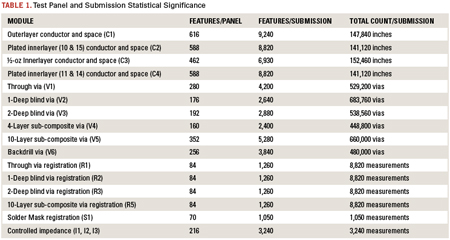
Beginning in 2006, we adopted the use of standardized test panels to quantify capability, process quality and product reliability of existing and potential ATE board suppliers. The test panel design was selected to align with typical ATE board requirements. It is a 24-layer, multi-lamination build using an 18" x 24" (457.2 x 609.6mm) panel. It incorporates six via types, each built using two different drill diameters: through-hole, back drill through-hole, blind mechanical, buried mechanical, one-layer deep microvia, and two-layer deep microvia.
Test panels also include four plated-layer trace widths ranging from 0.003"-0.006" with three spacings of 0.004"-0.006." Four non-plated trace widths range from 0.002"-0.005" with three spacings of 0.003"-0.005." Controlled impedance is evaluated for 50Ω single-ended lines and 100Ω differential pairs on surface microstrip, embedded microstrip, and stripline. Coupons testing soldermask registration and conductive anodic filament are also utilized.
A test panel submission consists of 15 test panels manufactured in three equally-sized lots with no less than one week between the start of each lot. Requirements to achieve ATE board alignment include a target thickness of 0.187" (4.75mm), electroplated NiAu surface finish, and typically specified laminate materials. All manufacturing processes must reside within the facility producing the test panels. Disclosure is required if any outsourcing is used. Supplier results include quantifications in terms of defect densities as defects per million vias (DPMV) and defects per million inches (DPMI), percent registration yields, process variations as coefficient of variation (COV), capability potential (CP) and capability performance (Cpk), thermal cycles to 10% resistance change / open circuit, and hours to conductive anodic filament (CAF) failure.
Table 1 highlights the number of features both on this test panel design and the full submission quantity.
Suppliers are expected to complete the 15-panel set in about three months. Third-party testing takes one to two months to complete.
Latest Test Panel Study Results
Some notable observations from our supplier’s most recent test submissions include the following:
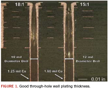
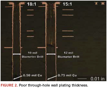
Via daisy-chain defects indicate 0.010" diameter, 18:1 aspect ratio through-hole vias continue to prove to be challenging for some suppliers.2 We found 0.012" diameter, 15:1 aspect ratio through-hole defects are better by a factor of at least three times, but results vary significantly among suppliers. Test panel cross-section photos revealed inadequate hole wall copper plating for both 18:1 and 15:1 aspect ratio through-holes in some cases. Figures 1and 2 are test panel cross-section examples of good and poor through-hole copper thickness.
Test panels place registration coupons at each corner and amid the central area. Through-hole registration results are provided in terms of percent yields within an allowed radial distance outside a 0.012" drill diameter. Radial distances in this case measure from 0.003" to 0.008" given in 0.001" increments. Test data expectedly show that results are significantly better at the center area of the panel. It may be desirable to consider central panel registration results vs. panel corner results separately, especially in cases when boards are fabricated far from the corners. Combining test results from all areas, the greatest supplier results range for 0.012" through-hole vias was at the 0.006" radial distance.
Thermal cycle testing is performed similarly on all via structures used in the panel design. After test coupons are subjected to six passes of a 260°C assembly simulation reflow profile, they are placed in an air-driven temperature cycling chamber that attains extremes between -40°C and 145°C.3 Next, 4-wire resistance measurements are taken across via daisy-chain structures during cycling. Specifically noted is the number of cycles until 10% resistance change and cycles to open circuit, defined as 20Ω or greater.
Test results show thermal cycle performance does not always correlate to defect density. A supplier may have good defect density results, but poor thermal cycling performance at the same time. Significant differences were demonstrated between the 18:1 and 15:1 aspect ratio vias. 15:1 aspect ratio through-holes attained at least two times the number of thermal cycles achieved by 18:1 aspect ratio vias.
Mechanical blind vias on this test panel are 10-layer, 0.008" and 0.010" drills with aspect ratios of 6:1 and 5:1, respectively. Mechanical buried vias are four-layer, 0.006" and 0.008" drills with aspect ratios of 3:1 and 2.5:1, respectively. All areas of blind and buried via testing, including defects per million vias, registration yields, coefficient of variation, and thermal cycling show significantly higher performance than the through-hole via test results from all suppliers.
Use of lower aspect ratio blind and buried vias combined with sequential lamination and lower through-hole aspect ratios is the preferred build method for ATE boards over the use of high aspect ratio through-hole vias and no sequential lamination cycles.4
One-layer deep microvias utilize 0.003" and 0.004" drills with aspect ratios of approximately 1:1 and 0.75:1, respectively. Two-layer deep microvias utilize 0.007" and 0.008" drills with aspect ratios of approximately 0.85:1 and 0.75:1, respectively. One-layer deep, 0.003" laser drill defect densities continue to be at least two times higher than the 0.004" drill. Supplier results range widely among both drill diameters.
Both two-layer deep microvia drill diameters have significantly better defect densities than the one-layer deep microvias, but supplier ranges still vary widely. There appears a correlation of better results when in-house laser drill is performed vs. outsourced laser drill. Outsourced laser drill is demonstrated to have acceptable results, but considerations in regard to where post-processing and plating is handled should be made, especially if buildup microvia layers are used.
Laser microvia thermal cycling results demonstrate much higher performance than through-hole vias, achieving similar results as the 10-layer mechanical blind vias. Conductor and space test results are provided for three different layer-types: plated outer layer, plated innerlayer and non-plated 0.5 oz. innerlayer. Plated outer-layers have a surface finish of electroplated NiAu specified at a minimum 200µin nickel underneath 5-15µin gold with Knoop hardness from 130-200. Plated innerlayers are a result of the sequential lamination build in this case and do not have a surface finish.
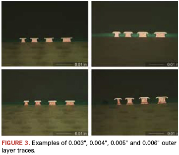
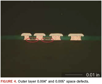
A conductor defect is simply a measurement of an open, and similarly a space defect is measurement of an adjacent short. Conductor defect densities on plated and non-plated inner-layers tended to be acceptably low, with a few supplier excursions seen on the smallest respective widths. Result ranges were observed to be much greater on the outer-layer conductor defects, especially with the smallest 0.003" trace width. Figure 3 shows four different supplier examples of the outer layer 0.003", 0.004", 0.005", and 0.006" conductors. Notably, significant differences are seen among all four examples in terms of copper trace etch factor, NiAu thickness, and length and shape of NiAu overhang.
More commonly encountered in ATE board development are space defects, especially when fine pitches are involved, and the test data reflect this. High supplier result ranges are observed on all layer types, especially at the smallest widths tested. Among all suppliers, the highest space defects occur on the plated outer layers. While defects per million inches is substantially highest with the 0.004" spacing and incrementally decreases by whole factors at both 0.005" and 0.006" spacings, very large ranges within supplier results are found on all outer layer space widths. Outer layer space defects were observed on test panel cross-sections (Figure 4).
Managing Test Results Data
After receipt of supplier analysis reports, two applications of the data used are a scoring system and design for manufacturability rules. Developing a scoring system for supplier test panel results is advantageous for many reasons. The number of test results for each individual supplier is extensive. Such a system can be used to simplify data analysis and supplier comparisons. Different scoring weights can be allocated to areas according to the greatest emphases for ATE boards. Ranges for acceptable high and low ends of test results should also be included. Scores are used to identify weak areas and promote competition among suppliers without revealing one’s specific test results to another. Board fabricators can be told non-subjectively where they placed among the supplier base. Allocating Weights
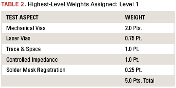
Level 1: The scoring system developed here is based on a 0 to 5 point overall scale. Many different test panel features, feature sizes, and test types require approaching the results on different levels. Level 1 represents the five highest test areas examined on this panel design: mechanical vias, laser vias, trace and space, controlled impedance and soldermask registration.
Based on the 5-point maximum, each area is allocated the weights shown in Table 2. Mechanically drilled vias are understood to be the weakest link in a high-performance ATE board and receive 40% of the total points. Trace and space and controlled impedance each get 20%, laser vias 15%, and soldermask registration 5%. Historically, soldermask registration capability has not strongly impacted ATE board development, but will likely become more important as component densities continue to increase.
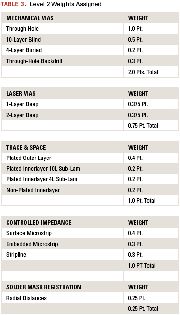
Level 2: Level 2 separates these five areas into their specific feature types. For example, mechanically-drilled vias comprise four different structures on this test panel design: through-holes, backdrill through-holes, 10-layer blind and 4-layer buried. Considerations for the amount of weight to apply to each feature type can include Difficulty to Produce, Frequency of Use, Susceptibility to Failure, and Supply Chain Availability. Table 3 is a breakdown of the five high-level test areas in terms of their feature types and shows the allocated weights assigned to each.
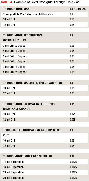
Level 3: Level 3 is the final level and involves specific test panel results. Feature types are further separated in Level 3 by two factors: Type of Test Performed and Feature Size. Six test types are considered for the through-hole vias: defects per million vias, registration, coefficient of variation, thermal cycles to 10% resistance change, thermal cycles to open circuit, and hours to CAF failure.
Considering the two through-hole drill sizes used, 0.010" and 0.012", 18 total test results are applied here for the through-hole feature type. Table 4 is an example of the Level 3 weights assigned for the through-hole via feature type. As with Level 1 and Level 2, weight allocations for specific test types and feature sizes can be based on several factors. In this example, the test types of defect density and registration are each allocated 30% of the total weight, thermal cycling 25%, process variation 10%, and CAF 5%.
All different feature sizes have their allocated weights split evenly in this example, but that does not have to be the case. Emphasis may be placed on feature sizes more difficult to produce or perhaps feature sizes most commonly used.
After weights are assigned to all individual tests, acceptable test result ranges are indicated and used to determine the supplier’s score on a specific test. A supplier’s result is compared against the acceptable range, and then a weight factor is determined. The weight factor is based on where the test result falls within the acceptable range.
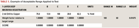
Table 5 is an example of the 0.002" radial distance microvia registration for the one-layer deep feature. Here, five supplier test results are shown as A-E. The allocated weight for this test is 0.01875 points, and the specified acceptable range is 60% to 100% yield. In this case, the target is a maximum 100% yield. If a supplier achieves the target result or better, the entirety of the allocated weight is awarded. If the test result is at the farthest end of the specified range or worse, the supplier receives no score. When the result falls somewhere within the acceptable range, the supplier receives a percentage of the allocated weight determined by position within the range. In the example, a test result of 70% yield would earn 0.25 times the allocated weight; 80% yield would earn half, and 90% yield would earn 0.75 times the allocated weight.
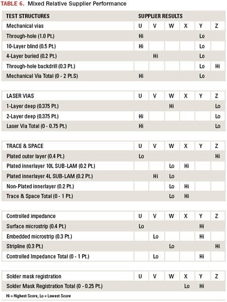
This scoring system is applied to a total of 212 test results for each supplier. Table 6 depicts highest and lowest scores achieved at Level 2 for six suppliers using color coding. Ranges between high and low scores are appreciable in all cases. The table demonstrates that no single supplier exceeds nor fails in all test aspects.
ATE Board DfM
Supplier test results can also be used as the basis for a DfM rule-set. When a multi-supplier strategy is incorporated, test results can certainly be used to determine recommended suppliers based on specific board build requirements. DfM rules should be implemented globally however. This ensures board designs are not limited to single-source manufacturability or perhaps a very limited number of suppliers. Whenever possible, the same aspect should apply such that novel, single-source technology capabilities are avoided if at all possible. DfM minimum and maximum constraints are used to establish quantified limits for improving fabrication yields. Whenever a design allows, absolute minimums and maximums should always be avoided and the number of their occurrences limited.
Mechanically drilled vias with high aspect ratios. As noted earlier, mechanically drilled vias with high aspect ratios have implications that go well beyond a supplier’s ability to merely produce them. This is considered to be the most critical DfM rule to be specified for ATE boards.5 Prohibition of techniques such as flip-drilling, used to attain very high aspect ratio vias, might also be considered. Regardless of how well a supplier can demonstrate the ability of such a process, the result is still a very high aspect ratio via requiring sufficient plating thickness.
Maximum laser drill microvia aspect ratio. Most suppliers specify a capability range between 0.7:1 and 1:1, with 1:1 commonly identified as “engineering level”.
Prohibit mechanical depth drilling for plated vias. The technique of creating blind vias without drilling entirely through a board has proven to yield very poor results in terms of defect density, process variation, and thermal cycling.
Mechanical drill hole wall to hole wall spacing. Drill wander, material properties, wicking, and susceptibility to CAF failure are some considerations in determining this specification.
Mechanical drill hole wall to copper feature spacing. This specification should vary depending on the depth of drilling involved. Test panel registration results provide a good basis for this.
Laser drill hole wall to copper feature spacing. Test results indicate a significantly smaller spacing is feasible among most suppliers than with minimum mechanical drill hole wall to copper feature spacing.
Copper feature to copper feature spacing. Fabricators may indicate this capability as a general minimum to be applied within an entire board, but supplier test results indicate consideration may be necessary for different cases of plated outer layer, plated innerlayer, and non-plated innerlayer.
Supplier Improvement Trends
After test panel data is received, supplier debriefs completed, and improvement plans are communicated, a common question is, Are the board fabrication suppliers getting better? Charts of average defect density trends for through-hole, blind, buried, and laser microvias all indicate supplier improvements. The following graphs represent our specific supplier test panel submissions. It should be noted they are not a representation of the entire PCQR2 database and all suppliers that participated within it.
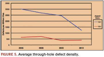
Figure 5 shows that average supplier 18:1 aspect ratio through-hole DpMV has decreased since 2006 from a high of 3,009 to 1,234 from the latest test submissions. Average 15:1 aspect ratio through-hole DpMV ranged from highs of 643 and 708 in 2006 and 2008, respectively, to lows of 375 and 402 DpMV in 2009 and 2010, respectively.
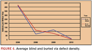
Figure 6 shows 10-layer, 0.008" blind vias had an average supplier defect density of 416 DpMV in 2006. This decreased to 11 DpMV by 2010. For four-layer PCBs with 0.006” buried vias, the average supplier defect density was 425 DpMV in 2006, decreasing to 5 DpMV by 2010.
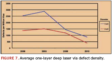
Finally, 0.003", one-layer deep microvia DpMV fell from a supplier average peak of 2,882 in 2008 to 867 DpMV in 2010 (Figure 7). And 0.004", one-layer deep microvia DpMV fell from an average peak of 1,512 in 2008 to 395 in 2010.
Conclusions
Benchmarking and qualifying PCB fabricators for semiconductor test boards requires a quantitative, statistically significant approach that otherwise invites unacceptable risk. Standardized test panels provide a sound basis for engaging with the supplier base and participating in continuous improvement plans. Over time, test panel results objectively demonstrate if suppliers are attaining agreed-upon goals. Since the test panels are close representations of the end-product, it is reasonable that measured process capability, quality and reliability improvements directly impact the fabrication of our ATE platform boards, contributing to maximum entitlement of semiconductor device manufacturing.
Acknowledgments
The author would like to acknowledge the support of Texas Instruments in this ongoing effort, and thank you to Mike Korson in particular. Thanks also to Norm Armendariz, John Hite, Pete Profilet, Martin Gao, Stan Ferrell, Jim Oborny and Marc Mydill. The author would like to acknowledge and thank the support of David Wolf and Tim Estes of Conductor Analysis Technologies. Special thanks to the IPC PCQR2 Database D-36 Subcommittee and all Texas Instruments’ ATE platform board fabricators.
References
1. D.L. Wolf, “Via Reliability – A Holistic Process Approach,” SMTA International, October 2009. 2. Bill Mack, “Benchmarking Printed Circuit Board Fabrication Suppliers Using IPC’s PCQR2 Database,” Burn-in & Test Socket Workshop Proceedings, March 2007. 3. IPC-9151C, “Printed Board Process Capability, Quality, and Relative Reliability (PCQR2) Benchmark Test Standard and Database,” May 2010. 4. Kevin T. Knadle and Virendra R. Jadhav, “Proof is in the PTH – Assuring Via Reliability from Chip Carriers to Thick Printed Wiring Boards,” Electronic Components and Technology Conference, June 2005. 5. Kevin Knadle, “Reliability and Failure Mechanisms of Laminate Substrates in a Pb-free World,” IPC Apex Expo, March 2009.
Ed.: This paper was first presented at SMTA International in October 2011 and is reprinted here with permission of the author.
Multi-Fineline Electronix (MFLEX) and AT&S last week announced an agreement to share their respective printed circuit board technologies. Under the agreement, AT&S's high-density interconnect (HDI) rigid PCBs and MFLEX's flex board capabilities will be offered to respective customers, and the two will partner on rigid-flex technology.
MLFEX executive and PCD&F columnist Jay Desai spoke with editor-in-chief Mike Buetow about the new partnership.
Read more: ‘An End-to-End Solution for Assembled HDI Rigid-Flex’
Nothing revealed shook the industry, but after a year of natural disasters, that was a good thing.
If Productronica is, as many believe, the bellwether for the printed circuit board industry’s health, 2012 should shape up better than most prognosticators are currently forecasting. Although the annual Internepcon and JPCA Show in Tokyo are larger, at least in attendance, Productronica remains the de facto prism through which the industry is observed.
Traffic at the biennial trade show in Munich was busier than in 2009, with event organizer Messe reporting attendance up 34% to about 34,000. That’s still below 2007, when it was a reported 40,000, but welcome news nevertheless. Traffic was slow on the first day, but very busy the next two, before tapering on the final day.
Compared to 2009, the physical show itself seemed smaller – and this is relative, as it remains bigger than almost all the other major electronics assembly trade shows combined – with traditional powerhouses like Siemens, Universal Instruments and other placement companies occupying booths that, while they would still qualify as monstrous at any other show, no longer fill entire halls on their own. (This is a good thing.)
For its part, Messe reported the total exhibit space was larger, but we think it was dissembling; several large lounges on the show floor were there to fill holes. Plus, we recall when the U-Bahn stopped at both entrances of the massive New Munich Trade Fair Center; this year, the East entrance to the hall was no longer needed. Productronica is shaping up primarily as an assembly and test show, with roughly one of its halls devoted to fabrication and bits and pieces of other industries (backend packaging, plastics, solar, EMS) mixed in. Most equipment advances seen were evolutionary, with incremental improvements in speed and accuracy. There were perhaps a dozen EMS companies, mostly Germany-based. Most are heavy into serving the industrial end-markets. All but one suggested that 2012 would be flat. For additional color, we were looking forward to the CEO roundtable late Tuesday morning, but as it turned out, the event was held in German. Verflucht!
Material Issues
Comments regarding low-Ag solders were cheap and plentiful. Most solder vendors agree that, despite the lower cost, assemblers find having to perform yet another round of alloy testing a turnoff. Moreover, there are questions over the applications for which they are best suited. Europe is pushing for nonflammable alternatives to freezer sprays. Europe and the US are not in sync when it comes to MSDS standards. Europe has standardized on a form, while the US is coming under fire for failing to do the same. AIM showed its NC258 no-clean solder paste, which debuted earlier last year. Electrolube displayed an array of new sprays and coatings, many driven by REACH requirements. Likewise, Henkel had a new paste and flux, the Pb- and halogen-free Multicore HF200 solder and halogen-free, no-clean MF390HR flux, and two new adhesives: Ablestik ICP-3535M1, a single-component electrically conductive adhesive and ICP-400, a conductive silicone. Senju rolled out the M40 line of low-Ag paste, but a representative said its industry outlook for 2012 is poor.
Asymtek named as president Peter Bierhuis, formerly president of March Plasma. PVA showed a pneumatic pump, DPCC, said to reduce air pressure on the conformal coating fluid reservoir and thereby prevent bubbles from forming. It can be installed on the new PVA6000 coater and dispenser. They also mentioned a trend toward solvent-based conformal coatings and higher flow underfill. Ersa debuted the F1 screen and stencil printer.
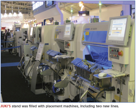
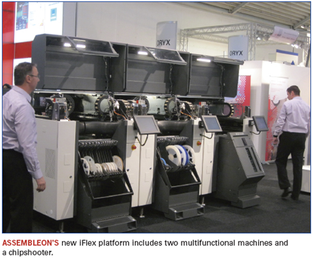
Placement OEMs are always the highlight of Productronica, and none of them would consider skipping this show. Juki showed several new machines, including the KE-3010, a high-speed placement machine capable of 80,500 cph per IPC-9850, and the KE-3020V, which handles everything from 01005 to 50 x 150mm and 75 sq. mm parts. Assembléon debuted a multifunctional platform called the iFlex, which potentially would compete with the Yamaha lines it has for years distributed. For its part, Yamaha has been gearing up to establish a direct US and Europe sales and service presence, hiring staff (including GM Scott Zerkle, formerly of Assembléon) and developing a new North America channel with one of its longtime Asian distributors, Transtech. Samsung showed its new SLM 110 Smart LED mounter, a dual-head machine with a patent-pending feeder. Universal debuted its latest Genesis pick-and-place machine, GC-120Q.
Ersa released two soldering lines, including the small-sized EcoSelect 1 selective soldering machine, and a hybrid rework system, the HR600. IBL showed several vapor phase machines, including a new inline model, the CX600. SMT-Wertheim showed its QP-L-Plus reflow oven. Vitronics has sorted out its production; wave machines are being made in China, reflow in US, and selective in Netherlands.
There was at least one potentially significant cleaning advancement: Speedline Technologies introduced its first batch cleaner, the Aquastorm 50, which uses patent-pending technologies common to the Aquastorm 100 and 200 inline cleaners to deliver dynamic energy to the board. The system’s rinse control reportedly guarantees desired board conductivity, and the drying technologies dry product to 0.1g of prewash weight. It is expected to be introduced in the US this quarter and elsewhere in the June quarter. Aqueous Technologies CEO Mike Konrad revealed 85% of its customers are cleaning no-clean flux. Zestron introduced Vigon N, a flux residue cleaner. After attending graduate school and spending several years running its US operations, Zestron CEO Harald Wack has settled back in Germany with no issues. Kyzen debuted the E5321 alkaline cleaner for pallets and general maintenance.
BPM Microsystems’ Model 4800 automated device programmer line can now program 36 devices concurrently, including all types of flash memory. Data I/O had its RoadRunner 3 automated inline chip programmer, which connects to MES or other shop-floor control and ERP software, including Aegis, with whom Data I/O just inked an agreement.
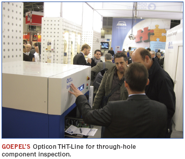
Goepel’s Opticon 3D x-ray offered real-time multi-angle image recording at test speeds of 40cm²/s. Meanwhile, the Opticon AOI can handle up to 32 devices under test simultaneously using a top camera and bottom-side scanner. Viscom mentioned its Europe and North America markets have been strong. The company is marketing Viscom as the sole inspection company that covers all test gates, from wirebond to assembled component. Mirtec exhibited its latest benchtop enhancement, the MV-3 AOI, featuring one top-down and four angled 10 MP cameras. Vitrox showed the 510XL x-ray, which handles maximum board sizes of 610 by 610mm (24 x 24"). Dage debuted X Plane technology, a software tool that mixes certain component adjustments, retrofits and new software in order to separate the component package, wirebond and board layers to reveal voids and other hidden defects. While solder volume characterizations are not possible, it was suggested they are potentially not far away. A rumor began, then subsided, over Koh Young’s patents on dual lighting. The patents have been challenged in several nations as being overly broad. Koh Young reports courts in Korea and China have upheld the patents, however. DJ Tech, the Japanese AOI company, showed a 2D/3D SPI. Acculogic had the Flying Scorpion FLS980 DXi double-sided probe tester.
Etek Europe has moved into its new $1 million headquarters. The Scotland-based distributor has added 14 staff in the past 18 months and is adding a demo room and possibly IPC training. It also has registered Etek USA. Managing director Mike Nelson did not sound like Etek will come to the US in the near term, but it could be on the horizon.
Rise of the Robots
The PCB fabrication exhibits have shrunk over the years and are now down to about one hall (although exhibitors were spread over two, intermingled with large lounge areas and contract assemblers). Like the (much bigger) assembly sections, exhibitors felt Tuesday’s traffic was slow, but Wednesday and Thursday were strong. Ten years ago, Productronica featured lots of large plating and develop/etch/strip lines and lamination equipment designed for large and heavy backplanes. Meanwhile, machines shown at the CPCA Show in Shanghai could fit in a shoebox. That equation has completely flipped: Productronica is now characterized by ample models of small-scale prototype and batch production equipment. Still, the number and quality of lines far outpaces that of all other Western shows (namely IPC Apex/Expo). Notable for its absence was Hitachi, the world’s largest PCB drill supplier. Nor did we see any laser drills onsite.
In the fabrication halls, robotics were the rage. Around 2000, sensors seemingly overnight showed up in almost all equipment. We witnessed perhaps the beginning of a similar surge in robotics: Several systems had robotic arms or handlers, including Kuttler’s Cleanline loader.
Most major laminate and material vendors were there, including Kingboard, Isola, Nelco, Rogers, ITEQ, OMG, Uyemura, Dow and others. There was a difference of opinion as to how important halogen-free materials are today, with some vendors asserting they are of low priority and others (Shengyi Tech, for one) indicating high demand, especially in Japan and Europe. Many echoed Arlon, which said it saw plenty of demand for high-temperature materials. ITEQ sees business flattening, while others willing to comment were slightly-to-somewhat more positive. Most felt the next two or three quarters would be bumpy, and there were complaints of Chinese knockoffs of raw materials and finished laminate. The good news is that shortages of glass and other raw materials brought about by the March earthquake in Japan have receded.
Isola said its high-speed digital business is growing, and the company is adding capacity in Taiwan. Rogers was busy, with customers mainly from Germany and Europe. Shengyi Tech said lead times are stable. Kingboard noted higher interest in Pb-free laminate materials. CCI Eurolam shared a booth with Isola, whom it distributes in Europe. It showed its Zetalam base materials.
Italian OEM Chemplate showed its Indubond 130N inductive bonding machine, said to facilitate pin registration for printed circuit board innerlayers. Bungard showed new lamination, UV exposure and drill and route machines. Dave Howard said 2011 was a record year for Bürkle, buoyed by a strong first half in photovoltaic and other non-PCB equipment sales, but he did not seem as optimistic about 2012. CA Picard agreed that after 18 strong months, the market has been quieting down since September. Dynachem has introduced two new machines in the past two years, including a new cut-sheet laminator, the SmartLam 5000. Activity was hopping at Kuttler Automation, which displayed a new Mylar peeler (P650), featuring an optical-based off-center adjustment. It also reported on, but did not have at the show, a new copper recovery system.
It is remarkable how many Germany-based equipment manufacturers remain, even though the continent has seen its bare board industry decimated. (It’s more or less AT&S and then everyone else.) Walter Lemmen, another of the miniature line makers, had a UV LED maskless lithography machine and a compact final finish line (named, appropriately, Compacta). Posalux sold a drill to HMP. Lenz had a CNC drill and router. LPKF said the show was busy, with interest from both the fabrication and assembly side.
Orbotech’s booth was busy, in part because of its success in the LDI market. Miva has a new photoplotter and direct imager aimed at low-volume and prototype markets. Apollon-DI had a UV-LED direct imager.
Known for its continuous plating lines, PAL had no equipment to show because most US and European fabricators use batch plating. Pola e Massa had some robotic advancements to its wet processing and handling equipment.
Atotech shows several new products ranging from via fill to photoresist adhesion materials to the Touchless Transport System, which offers lateral guided transport of touch-sensitive surface, such as embedded circuits for its Uniplate systems. FujiFilm is expected to announce Multiline as its distributor in Europe. Interest in white solder mask is growing, especially for LEDs.
Polymer Ag had a slick new cross-sectioning system for laser-drilled holes. The aptly named Micro Hole Cross Sectioning sections holes down to 0.003" starting from the center of the via, and can lop a two-hours-long manual process down to about 4 min. Luther+Maelzer showed the A5 flying probe tester. Lloyd Doyle is a shell of its former self.
Unlike PCB assembly, Eastern Europe has been slow to adopt or attract fabrication. When asked, most exhibitors pointed to the region’s lack of process knowledge. 2011 likely will go down as a transitory year. Business dropped from the big rebound in 2010, but not so much as to call it a recession. By and large, the electronics design and manufacturing industry outpaced the broader economies, a testament to tighter business and process management. Yet the supply chain had to deal with multiple significant disruptions, and all these vectors will influence changes in the years to come. News out of Bangkok was that the waters rose so high, some factories were soaked on their second floors. Expect a big wave of new machines to replace the thousands lost in the flood. This should help give the equipment industry a bit of a reprieve from a slowdown that is expected to last at least three quarters. Some placement companies reported receiving more than 100 orders to date.
Also, the big drop in the solar market will claim many victims. Some think, once the bloodletting is over, there will be only a handful of companies left. Others aren’t so dire, but the clear consensus is that there is tremendous overcapacity in solar (estimates run north of 35%), and that it will be two to three years before demand and supply reach equilibrium again. In the meantime, expect companies as varied as DEK, BTU and Bürkle, plus a host of materials vendors, to spend more time concentrating on SMT again.
Behind a growing Santa Clara, CA, board shop that is setting the bar for quick turns.
Even those who remember Data Circuit Systems, the Silicon Valley printed circuit board fabricator that was built up and sold to Merix in 2004, might not realize a similar arc is taking place today.
Founded in 1977, Advanced Printed Circuit Technology has been owned and managed since June 2008 by former Data Circuit executives Steve Robinson, Ed Barclay and Bill Boyle. The company, which operates a 100-employee, 35,000 sq. ft. facility in Santa Clara, now has sales in the $15 million range and has set a goal of reaching $25 million in annual revenues – on par with Data Circuit prior to its sale.
With Robinson running the factory as president, Barclay handling the back room as CFO, and Boyle out in front of customers as executive vice president of sales and marketing, APCT has already come a long way toward meeting that mark. The company has poured millions into its personnel and equipment, including the first Maskless Lithography imaging line. The owners convened in December for a roundtable with PCD&F Editor in Chief Mike Buetow to discuss their quickturn model, which now permits 24-hour turns on 20-plus layer boards.
Q. Given the success the management team has in building up (and selling Data Circuit), how do you find the energy to try to repeat that effort? SR: After the success we experienced at Data Circuit Systems, we knew that we had a business model that customers found valuable and important. Finding the energy is very easy when you truly believe in your direction. This thought process has an amazing effect in developing a positive management team. We knew we had the experience; we knew we had the assets and manufacturing location, and we knew we had the talent in our personnel. Once those ingredients were in place, we were positive of a successful outcome.
BB: Data Circuit was hugely successful. We learned exactly what to do – and what not to do – with that model.
Q. Data Circuits was known for its extremely quick turns. Is APCT attempting to duplicate that model?
SR: APCT has already achieved an excellent reputation for the manufacturing and delivery of advanced technology product in one- to five-day cycle times. We took the model developed at Data Circuit Systems and enhanced it, ensuring APCT would be more efficient, with lead times and technology. The APCT facility is designed specifically for rapid response manufacturing; therefore, it is reflected in our capabilities and quality.
Q: Why is that the right model for APCT?
BB: When we manufacture product in 24 to 72 hours, it becomes a very valuable model to Silicon Valley companies. This is primarily proof of design product, and allows us to create many new customers. APCT has the capability of building boards faster than anyone in the country. The technology level is extremely high and may be the only model I believe will work in this country.
SR: I think the thing we learned from Data Circuit and transitioned here is to understand the customer’s need and satisfy that need. That need may be two panels of 24 layers in two days. Or it may be 500 panels of eight layers in three or four days. We do a lot of very large orders, but in very compressed cycle times. We are niche-focused in the quickturn segment for the reason we feel it is absolutely US-centric. But that quickturn segment is one to three days, not three to five days. There are now a handful of offshore suppliers that can support a five-day build.
We provide our customers with a solution. If we feel we can successfully build it, we build it. The culture is all customers are important. We find a tremendous amount of market share – we capture six to 12 new accounts per month – because [customers] don’t feel consistently supported by their current supply chain. We treat every order with the same level of service and commitment. That philosophy breeds immense customer loyalty. And I hear that a lot. Customers perceive such a high level of satisfaction from what we provide. We fail – everyone does – but it’s never out of a lack of effort or commitment to the program. We provide upfront support from sales to engineering to financing. The whole package is user-friendly.
BB: One thing that is unusual was a few months ago we received a large order from a medical company after building their “proof of design” volumes. Once tested they placed 12,000 pieces each of an eight- and 10-layer board with us. That normally would not happen in this country, primarily due to the pricing advantage from China.
Q. The decision to buy APCT came as the US PCB fabrication market was in a tailspin. Was there ever a point where you thought it might not have been a good decision?
BB: In all fairness, the purchase of APCT took place just prior to the tailspin that placed our entire industry in jeopardy. Our initial outlook as explained was very positive. As the slowdown deepened, like many other business owners we questioned our timing, but also understood that failure was not an option. We believed in our business model and understood the economic challenges that were associated with executing our plan. As things turned, our model was validated and APCT enjoyed significant growth during that 2008-09 time frame.
Q. Are you taking any different approaches to running a board shop this time around? If so, what’s changed?
SR: We have continued with our commitment to the culture and the visions that fostered the previous success we have enjoyed as individuals and as a company. We have refined those visions, and as a result, the company is outperforming our own aggressive goals. We continue to believe in the unwavering support to both our internal and external customers.
Q: How do you foment that culture?
BB: For sales, we look for passion and commitment. There are a lot of professionals out there, but not many with the passion to succeed. I can teach people how to sell; we can introduce you to customers, but I can’t teach passion. If you have that passion, you will be hugely successful at APCT.
SR: From an operations aspect, I think passion and culture go hand in hand. Our company doesn’t have a weekly plan; our plans change hourly. We term it, “How do you work with your hair on fire?” You have to be able to hear the truth and be brutally honest. You have to have a sense of urgency, not be a plodder. We want educated and calculated decisions to be made. We don’t emphasize experience, but it’s nice. But we find many experienced workers have habits we have to break – such as hesitancy and an unwillingness to make a decision. Our final decision [to hire] is always based on the person’s personality. Do they fit the team environment and do what the customer asks on that particular day?
EB: Those factors are very important. That sense of urgency is very important to us. Workers have to understand, whatever the customer needs, we are going to make that happen. The other important aspect is that they understand the concept of “team.” That is crucial to us. We support each other no matter what.
Q. You have invested considerably in equipment, including the new Maskless Lithography imaging line. What was the driver behind that decision? And on what basis are decisions on new or unproven technologies made?
SR: Yes, we have invested significant capital since acquiring APCT. Our commitment to provide leading-edge cycle times and technologies to customers continues to drive investments that include multiple AOI systems, multiple flying probe systems, vacuum lamination presses, ink jet legend printers and vast shop improvements. The Maskless Lithography Imaging System is the most recent investment, but is far from unproven. Our engineering team has worked side-by-side with the OEM to further develop this technology. The months of diligence have proven to be invaluable to both APCT and the Maskless engineering group. This testing has resulted in significant improvements supporting a major step in cycle time reduction and technology now available at APCT.
Q. The US supply base has been decimated over the past decade. What practices have you put in place to ensure access to a steady, reliable supply of spare parts and raw materials?
SR: While it is true that the US printed circuit industry has been decimated over the last decade, APCT insists on using the most advanced equipment and materials readily available. In fact, many of these suppliers are used throughout the country and around the world, therefore eliminating any questionable supply chain variances.
Q: How is the capex budget set? Do you have a set percentage of sales that you plow back into capex?
EB: We look at the critical areas that need improvement. It’s not based on a percentage of sales, but how we can change and improve our technology. As a history, the factory has some old equipment. In the last year, we’ve spent $1.2 million on capex. We made very sizeable changes in technology. In 2012 we will put in another $1 million in some key critical areas. It’s based on the market, what we have to perform to, and how we can make new products.
SR: We meet a lot to discuss customer trends and demand trends. Many recent meetings have been cycle-time driven. The technology was limited, and we continued to get feedback that OEMs were limited in their supply chain to the DDIs and TTMs that could provide medium technology. We fund most of capex out of cash flow. Process redundancy is another driver; downtime is not an option for short-cycle manufacturer. That’s been part of the three-year plan. Capital is customer-driven. We’ll probably always be in the 5 to 7% minimum range of revenue.
BB: I always want to understand what technology our customers are looking for next month and next year, and prepare for that. For example, we’re building stacked vias – we didn’t even dream of that a year ago, but it’s an up-and-comer and will drive revenue in the coming year. Q: How important is it to your model to have the latest and greatest equipment? SR: Our success has always been based on the people. A lot of manufacturers have all the toys, but can’t get out of their own way because they don’t have the right people. The direct imaging line is about cycle time and getting product to the floor. If you don’t have the right people driving that opportunity, you can be very inefficient and erratic.
EB: The other part is we believe in being leading edge, but not bleeding edge. The Maskless product is very much a technology that a lot of players have stood back from. We’ve done a lot of research on this, and it’s been in test for eight or nine months.
SR: We recently launched into production. The quickest turn we previously produced was three days for 20-plus layers. We were able to produce two orders above 18 layers in two days this week. We cut 10 hours in cycle-time out of imaging.
Q. Pricing and margin is at the top of everyone’s minds. Have you noticed any change in approach among customers insofar as ensuring you are sufficiently profitable to remain their long-term supplier, or is price still the prevailing factor?
BB: Pricing has always been and will remain an important topic. While margins continue to be very tight, our approach remains the same: Utilize the best equipment and people, along with highly controlled process parameters, which will reduce scrap and provide a cost-effective solution.
Q. California tends to be on the leading edge of environmental-related manufacturing restrictions. Do you find this a deterrent to doing business, or in this emerging era of traceability and extended liability, is this beginning to be a competitive advantage?
SR: There is no question that the state of California and specifically Santa Clara County requires each company to do their part in controlling any negative influence on our environment. APCT is committed to being a good neighbor and doing its part to support these environmental requirements. In addition, Silicon Valley is where much of today’s technology is developed, and we insist on being on the forefront of these technological breakthroughs.
Q. What makes APCT more capable or unique among its regional competition?
BB: We offer 24-hour turns on NPI, and our “ramp to volume” builds in three to five days, and we support low-cost volume requirements in three to five weeks, all from one contact, one call, one transaction. This capability allows our customers to take full advantage of the global market and capabilities with tremendous ease and without the cost of developing multiple suppliers.
EB: We bring a lot of experience from our frontline platers to our shippers. Our average tenure for hourly personal is seven to 10 years. That’s rare, I think. Our management and supervisor leadership is probably high teens or 20s.
SR: I think we’re a little spoiled at APCT because of our experience and our core people. We’ve met a lot of people who were supposedly gurus who, when they left, we knew they couldn’t work in our plating department, let alone in a management position.
Q: How fast can you turn a quote?
BB: Generally, if a customer requires, they can hold on the phone for a quote.
SR: We have made multiple shipments where the customer hasn’t even had time to process the purchase order.
Q: What level of access do your factory workers have to their customers?
BB: We encourage it. We have some DfM engineers on the phone all day, every day, with customers. Sometimes they are on the phone with the EMS customer’s customers. We love early involvement. On any delivery of less than 72 hours, we have a home contact number, so we don’t have to put a product on hold.
SR: CAM engineers, floor engineers, floor managers, leads … we have to have engineering and designer contacts. We have to have answers and get product moving. We don’t reference our quickturn business by days. We do it in hours.
Q. What are the five-year goals for the company? What internal metrics do you use to determine you are on the right track?
BB: APCT continues to strive for a minimum growth of 15% year-over-year and has successfully surpassed that goal each year. The company has a very detailed dashboard that gives management all the tools necessary to make the proper decisions in supporting our continued growth.
Q: Do you subscribe to the notion that America has lost its printed circuit board engineering edge?
BB: I personally do not.
SR: I think it depends on where you’re at. There’s no question there’s been attrition of good, smart people in our industry. But for us, in Silicon Valley, we’re a little sheltered, because this is a very active, technology-driving, state-of-the-art area. There are still a lot of really smart, really creative engineers in the CM, OEM and PCB manufacturing area in our region.
BB: I think we have the luxury of dealing with some of the finest designers and engineers in the country because we are located in the Silicon Valley. They come to us because they know what they want the board to do and don’t know how to achieve that. We help and support them with their decision-making.
Mike Buetow is Editor in Chief of PCD&F (pcdandf.com); This email address is being protected from spambots. You need JavaScript enabled to view it..


 , and dissipation factor,
  , determine signal propagation velocity, dispersion and attenuation. While these two parameters,