A new Web-based training program teaches cost-savings using best-of-breed design and purchasing practices.
Web-based instruction is a growing market, and developed correctly, offers many advantages over traditional classroom settings. A new comprehensive online workshop aimed at electronics designers and engineers is the first to focus specifically on industry-specific environmental considerations and compliance.
The rationale is clear: Some 80% of the environmental impact of a product occurs during design phase, says Technology Forecasters Inc. (techforecasters.com), which developed the tool.
The training program, DFE Online (techforecasters.com/dfe-online), is really a self-paced electronic workshop. Made up of eight modules, it combines voiceover narration with clear pictorials, drawings, text slides and even links to short, hosted videos to explain a variety of concepts related to designing electronics products for the least environmental impact.
“Designers and the product launch team need to understand the basics of efficient environmental design, so when they do it, they do it in the most efficient, cost-effective way,” explains Pamela J. Gordon, founder and president of TFI.
The developers did a good job considering how an engineer might best grasp and absorb information. Data and images are delivered in multiple formats. There’s even an optional quiz after each of the modules, to help ensure the participant understands the subject matter. If they answer 10 of the 12 questions correctly, a certificate is issued.
Topics range from hands-on engineering advice to the business cases for Design for Environment (DfE). They cover such aspects as toxicity, emissions and energy efficiency. At times, the detail is very specific.
The product disassembly module, for example, shows the process for choosing fasteners for disassembly. Diagrams and schematics detail best practices. Information on building checklists to ensure all the relevant considerations are made is included. The module also shows everything from sample designs to instructing on evaluating plastics, comparing plastics vs. metals, selling recycled product, and even creating new incremental revenue streams.
“We drill down pretty deeply to give engineers the kind of information they need,” said Dr. Harvey Stone. Stone developed the module on disassembly.
Each module has about two dozen videos or documentaries that are rated based by TFI on relevance. They feature interactive exercises, so users can see dynamically the impacts and tradeoffs of material, component and energy choices. Information on documentation is included. A nice touch is the built-in forum at the end of each module, which offers users a chance to interact, compare notes and ask questions.
The program is built to be used by more than just the environmental engineer at a large manufacturer. Designers, buyers, and other hardware engineers at any sized company will find much to choose from. And Gordon stresses that the DFE Online isn’t just a series of reminders to be green for green’s sake.
“There are a lot of economic points in here. Beyond the environment and worker safety,” she says, “it’s about streamlining the assembly process and making products that use less energy. It’s really about the bottom line.”
Indeed, an explanation of modular design shows how to leverage a “used” assembly so that it can be used across multiple products, a move that not only is a more efficient use of materials, but also saves on troubleshooting and component acquisition costs.
“Our experience is electronics products designers do care about the environment; they just don’t know what they can do to design a product to minimize environmental harm, while at the same time saving money for their companies,” Gordon explains. “They don’t always realize how to connect the things they do.”
Compliance with major regulations such as RoHS and WEEE is, of course, a major headache for many companies. It is addressed often, but as a thread inserted in each module, as opposed to as a standalone module.
The program is customizable: Managers can choose which slides a product team or customer should focus on. TFI offers DFE Online as a lifetime single or enterprise license ranging from $995 to $19,500, depending on the number of users.
Flexible printed circuits have emerged as a standalone industry, complete with dedicated purchasing teams.
Perhaps I’m being a bit bold, but I believe that not only have flexible printed circuits and assemblies (FPC/A) matured into their own industry, but they also have enabled a density of electronics that rigid PCBs cannot achieve on their own.
What trends might I see that support this notion? As my colleague Jay Desai has pointed out in past columns, thin is in. And flex assemblies deliver on that promise with high reliability. FPC/A has its own stable and large supply chain in the US, Japan, Taiwan, Korea and China. OEMs have dedicated FPC/A commodity managers. In fact, OEMs now expect FPC/A companies to do both flex and flex assembly – beyond just surface mount technology. Leading FPC/A companies know how to engineer and build in 3D, enabling and supporting the flexible interconnect and packaging solution from OEM concept design to mass production and functional test. Finally, we’ve been doing this for a decade now; this isn’t new. It’s mature, it’s automated, it’s laser-guided, high-technology FPC/A in mass volumes.
OK – time to pinch myself. From an engineer’s perspective, how much of this is visionary, and how much of this is actual, developed materials, process and applications that meet the current and future feature density of smartphones and tablets? Over the next year, I’ll answer those questions using evidence from new materials characteristics, examples of innovative applications of current and new technologies, and results of both characterized process and simulations that highlight the latest interconnect and packaging advantages FPC/A provides.
How did FPC/A get to where it is today? Flex circuit and assembly technology has grown into its own industry largely from its success as a critical component to smartphones and tablets. Portable devices have transformed not only the way the world communicates and interacts with data, but also the way we think of flex. FPC’s core ability to bend, fold and twist thin interconnect traces with high mechanical reliability enabled unique applications to emerge from simple board-to-board jumpers to high cycle-count dynamic constructions needed to produce thinner, stylish clamshell devices in mass volumes.
As dynamic applications dwindled and the dominant design moved to the iconic candy-bar form-factor – a non-dynamic application with larger, more power-hungry displays – why didn’t the complex-FPC/A market diminish as well? FPC/A manufacturers engineered and produced subassemblies and functional modules that could be placed improbably close to the surface and corners of a device, and connect those modules reliably to the main board, all while increasing available volume for bigger batteries and additional features.
A material difference. Dielectric materials have seen significant, progressive decreases in thickness over the past few years, from 25, to 18, to 12µm for current production volumes, and as low as 6µm for development work. To mass produce such thin materials, key suppliers made significant improvements in properties such as tensile modulus, moisture absorption, coefficient of thermal expansion, and dimensional stability.
Improvements in the thickness and ductility of copper foil, combined with the reduction in dielectric thickness, have enabled flex layers as thin as 32µm, or even 24µm. When compared to the thinnest mass-producible PCBs, the difference is 38µm – roughly double the thickness. Roll-to-roll equipment advancements greatly improved processing these materials and expanded the capability to make finer and finer traces at high yield.
Making new connections. Dimensional stability improvements and multilayer registration have enabled continued advancements in miniaturization and density. Components as small as 01005 (0.41 × 0.20mm) for passives and I/Os as dense as 0.40mm pitch BGA for packages are being assembled on FPC in production. Other assembly technologies such as anisotropic conductive film (ACF) bonding offer small-pitch, connector-less, flex-to-flex, flex-to-board, and flex-to-glass over small-pitch, large-area interconnect solutions. Designers now may place multiple functions onto a single flex, instead of connecting discrete modules to a main board.
As more modularization happened at the wafer package level, more packages with unique heights needed to be incorporated into devices. OEMs needed help designing outside the box. Integrated FPC/A design and early supplier involvement provided flex modules that we built, assembled, pre-bent, tested and sent to contract manufacturers to be crammed into nonlinear, non-rectangular spaces in the device, allowing OEMs to pack an amazing amount of electronics into smaller devices.
If you think about it, FPC/A manufacturers gave OEMs a reliable alternative to embedding components into PCBs, by maximizing the use of space outside the rigid board. This represents the fundamental change in thinking around the value of flex. Flex isn’t just for flexible features anymore.
What’s next? Future electronics devices won’t lose functionality. For high-end devices, even more functionality must be crammed into the same or smaller spaces. For lower-end devices, functionality has to be further integrated in order to reduce cost. Higher component density, better signal integrity at higher frequencies, and thinner overall circuits are needed, and at the same or lower overall device cost.
How might the FPC/A industry respond given the new, 3D way in which we think about flex? How might FPC/A companies use new materials and processes in both flex fabrication and assembly to provide mechanical and electrical performance solutions for the next generation of electronic devices?
I believe low-loss dielectrics and continued improvements in copper-trace structure may answer the higher-density, higher-frequency, and higher signal-integrity challenges. I believe that single- and double-sided assembly on flex with direct chip integration by flip chip or other circuit-level packaging technologies may answer some of the space and cost challenges with wafer-level packaging.
And I believe FPC/A will be used in future product designs more equally with rigid PCBs, enabling the next generation of electronics products.
Dale Wesselmann is a product marketing manager at MFLEX (mflex.com); This email address is being protected from spambots. You need JavaScript enabled to view it..
When thermal mismatches are to blame, what’s the cure?
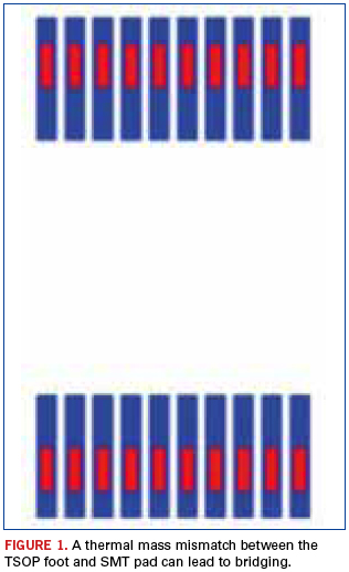
One root cause of bridging with TSOP components is a size mismatch between the TSOP (U2, 24-lead) and the SMT pads. Typically two problems are caused at reflow due to component-footprint mismatch: bridging and insufficient solder volume. Bridging is the result of a thermal mass mismatch between the pad and component lead, and most often occurs with gullwing devices. The foot (toe-to-heel) has a much smaller thermal mass than the pad and heats more quickly in the reflow oven. Molten solder will wet more aggressively to a hotter surface, so the majority of the solder volume pools at the toe and heel and does not evenly coat the pad and component lead. The gullwing lead cannot wet all of the excessive solder volume, and the excess flows off the SMT pad, bridging to the adjacent pad.
Insufficient solder volume is a result of too much surface area for the solder to wet to, and most often occurs with QFNs and RNETs. Since the surface area differences are not nearly as drastic as those with bridging, the temperatures of the SMT pad and the component terminations are much closer during reflow. As a result, solder evenly wets to both surfaces. However, a pad that is too large requires extra solder volume to evenly wet all surfaces and still create a Class III solder joint. Component shortages and substitutions, and poorly designed boards, can cause either, or both, of these problems.
For this board (Figure 1), the bridging with TSOP U2 is the result of a very small foot (red) and a very large SMT pad (blue). The foot length is 0.0246" and the SMT pad length is 0.069". The foot only covers 36% of the pad length. For a properly designed board, the foot should cover approximately 75% of the pad length. The foot is getting much hotter than the pad during reflow, and too much solder volume is pooling at the toe and heel. Solder is flowing off the pad, causing bridging.
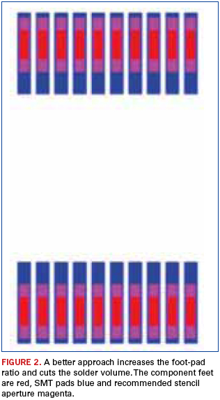
To eliminate bridging, the printed solder volume must be substantially reduced, given the very small component feet and the very large SMT pads. The recommended stencil aperture size is U2: 0.009" x 0.0485" (36% volume reduction).
Charles Robert Darwin communicated his theory of evolution more than 150 years ago. He observed some unique zoological evolutions while visiting the Galapagos Islands in Pacific Ocean during a global circumnavigation on a British research vessel name Beagle. Darwin recognized that each isolated island experienced its own evolution; each species developed a unique trait specific to that island. Darwin’s Theory of Evolution grew from these observations.
Read more: The Japanese Problem: Galapagos Syndrome
Component Placement “Two Worlds Converging: Chipshooting and Flip-chip Bonding” Authors: Eric Klaver and Patrick Huberts Abstract: Pick-and-place equipment has over the years mostly evolved in four key areas: It is faster, more reliable, more accurate and more user friendly. Most pick-and-place vendors have aimed at the mass production market, while others have moved toward more dedicated markets – mostly where production flexibility is needed, as with high-mix, prototyping or evaluation. But in the end, we’re all doing the same thing: picking and placing components on bare substrates. (Company white paper; circuitsassembly.com/cms/white-papers)
PCB Assembly “New Product Introduction” Authors: ASM Siplace Abstract: This new publication presents solutions for everyday challenges, lots of tips and tricks, and a convenient checklist for the NPI process. It is directed toward manufacturers that want to implement robust NPI processes in their high-mix electronics production environments with consistent tool chains in order to raise the efficiency and quality of their new product introductions. Readers will learn how even the first yield can be produced efficiently and error-free despite faulty Gerber data, incomplete bills of material, and missing or late component descriptions. (Company white paper; circuitsassembly.com/cms/white-papers)
Plating “Electrochemical Cell Geometry for Uniform Processing of Printed Circuit Boards” Authors: S.T. Snyder, H.M. Garich, B.S. Kagajwala and E. J. Taylor; This email address is being protected from spambots. You need JavaScript enabled to view it.. Abstract: An electrochemical cell geometry based on a novel flow mechanism for uniform processing (metallization or electroetching) of PCBs is described. This unique flow scheme utilizes eductors, coupled with dampening elements and flow channels to enable a non-impinging flow scheme that results in uniform boundary layer thickness and consequent uniform current and thickness distribution over a full-size printed circuit board panel (18×24 in.). This tank has been extensively characterized for thickness distribution under direct current plating conditions and compared with commercial plating cell geometries that utilize both eductor flow and/or air sparging agitation. Uniformity data, along with plating results of varying printed circuit board feature sizes, are also presented. (Products Finishing, August 2012)
“Immersion Gold: Why More is Not Better” Authors: Hank Lajoie and Trainor; This email address is being protected from spambots. You need JavaScript enabled to view it.. Abstract: The nature of immersion gold is to attack the electroless nickel, remove it and replace it for the benefits that gold can offer. This activity of gold can defeat the intent for its use and supports the approach, starting with gold is good, so more must be better. The ENIG process has been challenged with this “more is better” concept. The ENEPIG process attempts improvement with protecting the EN from the gold. The dynamic chemistries involved within the process require close control and proper balances of ingredients. The effects of some of these contaminations and process imbalances can be exacerbated through ignorance and neglect of process control and pursuing the “more is better” approach. Experience with these dynamics of the electroless nickel, electroless palladium and immersion gold have offered improved and robust chemistries that fit with practiced process controls and can realize the value of gold without the “more is better.” Effects of commonly encountered bath contaminations from materials, process environment and process controls are presented to illustrate the immersion gold impact on the electroless nickel that can lead to defects. (SMTA International, October 2012)
Soldering “Overcoming Head-in-Pillow Defects in Hybrid LGA Socket Assembly” Authors: Marie Cole, et al; This email address is being protected from spambots. You need JavaScript enabled to view it.. Abstract: The processor card of a new midrange server system has a unique large mass SMT connector system that requires use of a vapor phase reflow. In addition, the board contains four ball grid array connectors, known as hybrid LGA sockets, to accommodate plugging of LGA processors. Due to the large size of these BGA sockets, which makes them vulnerable to dynamic warpage and other physical changes during Pb-free processing, solder joints in the connector array may be more susceptible to the formation of HiP defects. This paper discusses optimization of the assembly process for this complex PCBA. Several design of experiments were evaluated, including solder paste chemistry, stencil parameters, vapor phase reflow profile settings, reflow SMT pallet and fixture designs. Additionally, characterization of the contribution of incoming connector tolerances and thermal dynamic warpage was considered, along with various reliability evaluations related to this type of head-in-pillow defect. (SMTA International, October 2012)
This column provides abstracts from recent industry conferences and company white papers. Our goal is to provide an added opportunity for readers to keep abreast of technology and business trends.
What is the downstream payback, and how will it inform solar use?
For the most part, this column has concentrated on technologies and processes used to raise the efficiency and lower the cost of photovoltaic (PV) cells. But have you thought a bit further downstream as to what that may mean in terms of how the cells will be used, the payback and, ultimately, the value to the homeowner? I’m guessing that a large percentage of you have not! (Come on, admit it.)
We are often so focused on a certain element of solar technology, that the bigger picture is overlooked. So, this month I thought it would be interesting to provide a general overview of residential PV systems – from installation to ROI to cell efficiency benefits to common myths. Perhaps after reading this, your roof will soon be the proud owner of some solar panels. The PV system and how it works. Understand the distinction between on-grid (or grid-connected) and off-grid (or non-grid-connected). On-grid systems are most common in areas of high population density and have connectivity to a local power supply. During peak/daylight hours, the homeowner draws what they need from the PV system and feeds the “extra” electricity generated into the national grid, for which there is a payout based on local Feed-in-Tariff rates. During the dark/off-peak hours, the homeowner draws power from the national grid. There are four main components to an on-grid system:
Solar modules (panels), made up of roughly 60 crystalline-silicon (c-Si) solar cells each.
Inverter used to convert the power from direct current (DC) to alternating current (AC) used by household appliances. (Note: Inverters may need periodic replacement, as they may not last as long as the panels.)
Regulator for voltage stability.
Meter to monitor the quantity of power the PV system is pushing to the national grid, so the homeowner can be compensated. A home that is completely off-grid is one that does not have easy accessibility to the nearest grid line. These systems are more popular in remote areas, where it is simply too expensive to provide the cables necessary to connect to the national power grid. In this case, the homeowner would have all the same components as the on-grid system, as well as:
Deep cycle lead-acid batteries that can withstand many deep discharge and recharge cycles.
A charge controller to ensure batteries receive the optimum charging voltage.
The batteries store power generated during daylight/peak hours, and the homeowner draws from the battery surplus in off-peak periods. Because of the battery requirement for off-grid systems, the investment is significantly greater than that of an on-grid system.
How many panels, how much power, what’s the cost and payback? Obviously, the quantity of panels required for a residential installation is dependent on a number of different factors, including the size of the home, average power consumption rates, orientation (sun facing or not) of the residence, roof tilt, on-grid or off-grid configuration and Feed-in-Tariff rates. Solar panels/modules are most commonly fabricated from approximately 60 c-Si solar cells, with each panel producing 200W to 250W peak. Anywhere from 12 to 15 panels are required to deliver a typical 3kWp system, which, generally speaking, will power a modest-size home (2000 – 2500 sq. ft.). Of course, if you have the roof space and the budget, a higher power system may also be appropriate. Using a typical English home as an example, one could purchase a budget/lower-end installation for a cost of around $9,400 or a deluxe/higher-end system for approximately $17,200.
With a modest solar PV panel installation (3kWp) positioned on an optimum roof configuration (south facing with a 30˚ tilt) in Birmingham, England, that was registered for the UK’s Feed-in-Tariff before Dec. 12, 2011, the homeowner could receive and save:
Annual tariff income generated: $1,600.
Annual fuel bill savings: $120.
Total income and savings: $1,890.
Projected net profit over 25 years: $27,700.
Expected time for full return on investment: 8 to 9 years for a $15,670 3kWp system.
On the other hand, if the homeowner were to have installed the same system and registered for the Feed-in-Tariff after Apr. 1, 2012, at the current, lower rate, the same scenario would result in the following:
Annual tariff income generated: $830.
Annual fuel bill savings: $120.
Total income and savings: $1,010 per year.
Expected net profit over 25 years: $7,580.
Expected time for full return on investment: 15 to 16 years for a $15,670 3kWp system.
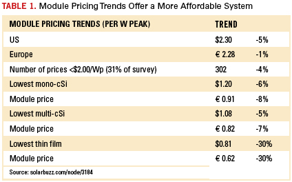
These examples certainly illustrate the massive impact that Feed-in-Tariff rates have on payback time and the effect that has on solar system adoption. Certain countries (read: Germany and Italy) had huge incentives for many years, making them the solar installation centers of the universe. With those subsidies now reduced, installations have slowed significantly. But, it’s not all bad news for solar. Solar system prices have simultaneously fallen dramatically due to several factors, the most significant of which is reduced incentive levels. In fact, the average cost of Chinese Tier-2 crystalline PV modules1 dropped to $0.96 per watt in January, representing an annualized price shift decline of 22%. So, while incentives may be lower, so are module costs (Table 1).
The efficiency equation. On the cell manufacturing side, there is a clear shift toward more efficiency, as opposed to more capacity. Instead of churning out average-rated 14% efficiency cells, there is certainly a move toward hitting the 18% to 19% efficiency mark, despite the higher cost. Obviously, the view is that more efficient systems will deliver a greater payback (fewer modules needed for the same energy generation), and, though the difference is slight at the moment, a more significant cost benefit is projected for the long-term.
The various technologies discussed previously in this column, such as print-on-print, rear-side passivation, MWT and selective emitter, all combine to substantially improve cell efficiency, thereby generating more power and ultimately lower the cost over the life of the system.
Solar fact or fiction. There are numerous myths about solar and its use as an alternative energy source, so I thought I’d take this opportunity to dispel a few.
Myth: “The energy required to make solar panels is greater than all the energy those panels will ever produce.”
Reality: The energy delivered over a 25-year period by a roof-mounted solar system in Central Northern Europe is roughly five times that of the energy required to make the panel.
Myth: “Solar panels work just as well when it’s cloudy.”
Reality: Solar panels will still work when it’s cloudy, but many of them will only produce 10% to 20% of their peak power. Before buying, it’s worth comparing the low light level performance of various panels. The panel datasheets usually show power graphs at several different light levels, ranging from the normal solar standard of 1000w/m2 to 250w/m2.
Myth: “Solar technology is improving so quickly that it must be better to wait before I buy.”
Reality: Small advances in cell efficiency do occur each year, but many countries are also reducing their Feed-in-Tariffs, so waiting may mean missing out on a good deal. Module prices are falling, so from that point of view, it may be worth waiting. But, for the overall cost of ownership, the Feed-in-Tariff is the real metric, and the longer you wait, the more likely this incentive will be lower.
Is there solar in your future? There’s no doubt that the solar industry is going through a bit of a reset at the moment, but for the long-term it is one of the most affordable and effective energy technologies and is no doubt here to stay. The majority of solar modules are guaranteed for 25 years and, at current Feed-in-Tariff rates, most homeowners realize complete ROI well before any modules need to be replaced. As new technologies continue to improve cell efficiencies, solar will only become an even better investment.
Tom Falcon is a senior process development specialist at DEK Solar (dek.com); This email address is being protected from spambots. You need JavaScript enabled to view it.. His column runs bimonthly.