
Silicon interposers competed with TSV at ECTC.
Gazing over the scenic San Diego harbor, more than a thousand people gathered at the Electronic Components and Technology Conference (ECTC) to discuss cutting-edge developments in electronics packaging, materials, and assembly.
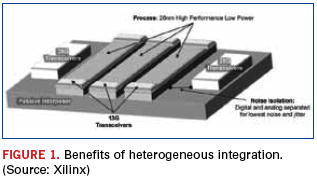
While crowds gathered for the numerous 3D through-silicon via (TSV) papers, an equal number of attendees focused on interposers – a solution that appears more near term. Papers from Altera, Cisco and Xilinx focused on product introductions and plans with silicon interposers. In an interactive session, Xilinx discussed its latest product, a 2.78Tb/s FPGA with serial connectivity – a heterogeneous solution combining three 28nm FPGA slices, two 40nm electrically isolated 28F transceiver devices, and 13G transceivers on a 65nm passive interposer (Figure 1). Cisco described a future solution featuring memory and logic on a passive interposer, while Altera’s solution will take advantage of TSMC’s chip-on-wafer (CoW) technology.
Remarkably, the structures look similar to what the industry called MCM-D or multichip modules (D is for a deposited thin film dielectric) more than 15 years ago. The major difference is that today’s interposers have TSVs, but some issues, such as ensuring a high-yield process is used to produce the substrate, mounting known-good die, thermal issues, and infrastructure, have not changed. Several companies discussed the possibility of using glass interposers and some discussed use of a laminate substrate with fine features instead of a glass or silicon structure.
The quest for 3D TSV. While 3D-TSV structures planned for immediate commercial production remain elusive, several presentations provided insight into structures on the horizon. Research institutes, including CEA LETI, various Fraunhofer organizations, IME, IMEC, ITRI, KAIST, RTI, and others, provided details of research underway.
Texas Instruments provided a look into its development work on an analog application with TSVs in a wafer-level package structure. Image sensor developments from CEA LETI and research partners NXP and ST Microelectronics showed a path from backside vias due to stacking in future image sensor applications.
GlobalFoundries CTO Gregg Bartlett provided one of the most compelling arguments for 3D TSV adoption during his luncheon keynote: the cost of future lithography systems for next-generation silicon node technologies, which tops $100 million. The promise of 3D TSV, with its advantages of improved interposer, bandwidth and latency, is as enticing as the vision of a harpy to a lost mariner – her cries drawing him into the jagged rocks near the coast. Whispered in the hallways during the conference were the trials and tribulations of the debond step in the wafer thinning process – required for both silicon interposers with TSVs and 3D TSV stacks. A number of material developments hold promise, but the peril of impact on yield remains.
Coreless substrates. Coreless substrates appear to be becoming a reality. A special evening session focused on advanced coreless substrate and material technologies from Japanese companies. Between sessions several substrate makers confirmed that demand for coreless substrates is increasing, and Intel provided details of its developments with a coreless substrate with controlled warpage – one of the big concerns that has slowed adoption of the structure.
Crowds jockey for a seat in Cu pillar sessions. Attendees crowded into standing-room-only presentations that focused on copper pillar developments. Presentations from foundries, OSATs and other companies clearly indicated the technology is becoming mainstream for more than just Intel. ASE, Amkor, STATS ChipPAC, SPIL, PTI and others discussed assembly progress. TSMC, now also playing the part of an assembly service provider, instead of just a foundry with bumping capability, provided a peak into its activities with Cu pillar.
Fan-out wafer-level packages (WLPs), embedded components, LEDs, MEMS and alternatives to gold wire bonding captivated the interest of attendees.
Many new material developments, especially related to underfill, were presented. Discussions of pre-applied underfill from materials suppliers and companies with applications were numerous. Increased use of Cu pillar appears to be one of the major drivers in the introduction of nonconductive films and pastes, with multiple presentations on the new formulations.
Planning is underway for next year’s ECTC, to be held in Las Vegas next May. Abstract submissions are due in October (ectc.net).
E. Jan Vardaman is president of TechSearch International (techsearchinc.com); This email address is being protected from spambots. You need JavaScript enabled to view it.. Her column appears bimonthly.


