The PCB designer is the architect for improved PCB yields.
A major requirement in improving board fabrication yields is doing
it right the first time, because once the PCB fabrication process is
complete there is really no way to go back to fix major mistakes. In
some cases you can mitigate design issues during the PCB assembly
process, but during PCB fabrication, once layers are laminated and the
holes are drilled, you cannot easily undo the process to make
corrections.
Therefore, to improve fabrication
yields during and after design layout, it’s critical to follow the
detailed fabrication notes and drawings, specifically calling out every
item that requires any kind of explanation. This includes stack up
data, layer construction information, material call outs, as well as
drill charts specifying hole counts and symbols, whether drill holes
are plated, and any similar information.
Notes and
drawings must not have sketchy or ambiguous information, nor should
they lead the PCB fabricator to make “guesstimates” about some of the
directions. Fabrication notes and drawings must have clear-cut and
precise information in their instructions – assumptions are not
allowed. If questions arise, the OEM customer should be consulted, and
the OEM should resolve any uncertainties.
A good rule
of thumb is to engage the fabrication house during PCB layout/design
stage. After the designer creates the stack up for impedance control,
it’s a good idea to get it verified before the files are released to
the fab house. Conversely, the fab house can play a reciprocal role by
providing the designer with recommendations and suggestions for
boosting yields. For example, a fab house may recommend material
changes for a specific application that are better suited to increasing
yields than those a designer specifies.
Also, it is
a good idea to check the capabilities of a fabrication house before
releasing a job to them. If the PCB design calls out for 3 mil lines
and spaces, and the fab house does not have the capability to generate
this type of feature, they can inadvertently over or under etch traces,
causing open or shorts resulting in yield issues. Therefore, working
together, the designer and fab house engineer can resolve any question,
issue, or ambiguity that arises at an early stage in the design
process, before the design ever reaches the fabrication floor.
The Importance of Fabrication Drawing
The
PCB designer is the lynchpin for improving fabrication yields from the
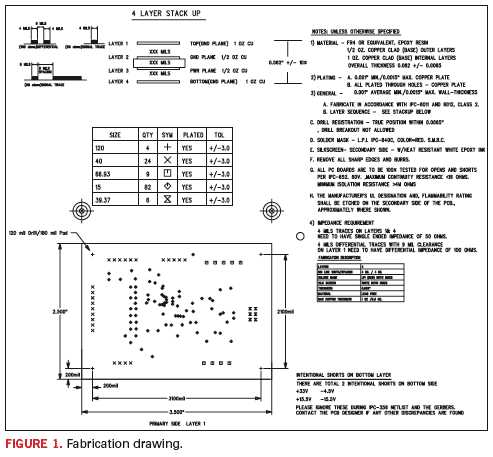
start. The fabrication drawing – the result of the PCB layout/design –
is the tool they rely on to achieve this objective. A seasoned designer
always finishes their layout by providing a complete fabrication
drawing. An efficient fabrication drawing has four components – notes,
mechanical dimensions/drawings, stack up callouts, and a drill chart
seen in Figure 1.

Fabrication
notes include a wide range of technical details and instructions. The
more complete and accurate they are, the more likely that the
fabrication house will be able to produce the PCBs with requisite high
yields. The following are some of the critical areas that should be
covered in fab notes.
It is important to list the
IPC class (I, II, or III) on the fabrication notes. Also, the designer
should specify the required board materials and surface finishes such
as HASL (lead-free or tin-lead type), electroless nickel and immersion
gold (ENIG), immersion silver or tin. If it’s gold, what is the
quantity and type? A typical soldering applications might call for 3 to
5 microinches of gold over 150 to 200 microinches of nickel. A higher
thickness and different type of gold would be needed for specialized
applications such as wire bonding. The designer should also include,
whenever possible, a note designating a secondary (equivalent) material
and manufacturer name if the primary choice is not available at the
fabrication house. It may take a week or more to acquire material,
causing OEM product delivery delays. That’s the level of detail the
designer must include in their notes.
Ensuring that
automated optical inspection (AOI) is used is another critical step in
board fabrication. AOI checks inner layers to ensure there are no opens
or shorts on the board, and that layer-to-layer registration is
properly aligned. For example, a note to a fabricator can simply state:
“Please make sure Layers 2, 3, 5, and 6 are AOI verified before
laminating the layers.”
Solder mask information
must also be covered, including if a solder mask is required on one or
both sides of the board, halogen content considerations and also
designating the color of the solder mask. In addition, it is always a
good idea for the designer to mention a few preferred solder mask
manufacturers. Fabrication notes must also detail maximum warpage per
square inch that the designer will allow, and this should be in
accordance with IPC guidelines.
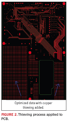
The designer also
should include a note on the thieving process that allows for even
copper distribution on the board. Thieving adds non-conductive copper
material to the board that balances copper weight on the board’s entire
surface, so that when etching is performed, it is uniform over the
board’s surface. This minimizes the creation of either opens or shorts.
Figure 2 shows a PCB design with copper thieving added.

Designing For Odd-Shaped Boards
When
it comes to fabrication notes, mechanical dimensions and drawings
require equal attention from the designer. This is especially true for
odd sized or unusually shaped boards that use radial angles to define
curvatures or slot dimensions. When creating a fabrication drawing for
such boards, the designer must specify even the smallest detail in
lengths, widths, and angles. The designer must carefully designate any
holes that reference each other, especially if they are at a specific
angle or run concurrent to each other.
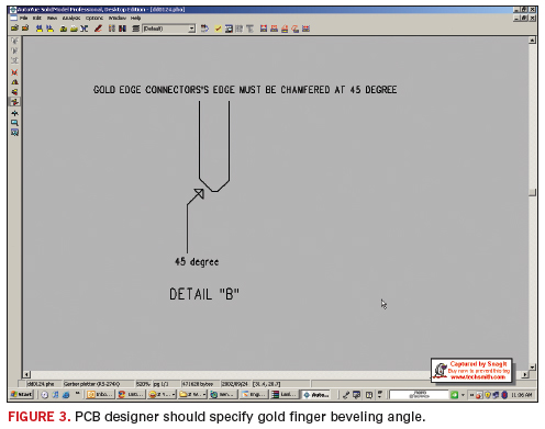
Gold
fingers, like cables and chassis wires, are used to connect daughter
cards to a motherboard or other subsystems, and when providing details
on the beveling of the gold fingers at the edge of the connectors, the
designer should specify the angle and at what levels the gold fingers
should be beveled (see Figure 3).

The
datum point 0,0 must be specified, so that every other dimension is
measured from that original point. Cutouts, slots, and holes must also
be meticulously designated. On the drawing, there are two sides for
reference designators. At times, the designer might note a special
feature on the bottom side that isn’t required on the top side. This
distinction must be made in the fabrication drawing. If not, the
fabrication house is left to make what perhaps can be a faulty
assumption. Other details the designer must include would be any
special features, like counter sink holes or sequential lamination.
Stack
up callouts specify board thickness, composition of internal layers,
pre-preg thickness, and copper ounces per square inch used on the
board. At the layout stage, the designer should perform precise
calculations on the amount of current that will flow through the board.
The callout specifies the thickness of copper (measured in ounces) to
comply with current requirements. What must be avoided is the
fabrication house relying on their own judgment, or making a decision
using no calculations at all. (Note: an “inaccurate judgment” is not
the fault of the fabricator, it’s a design error.)
When
calling out for impedance control requirements, a precise tolerance,
such as 5% or 10% should be specified. For high-speed designs,
impedance requirements could be single ended, or multiple differential
impedances. Since there are many factors that can change the impedance
on a board, a seasoned designer is always aware and mindful of these
factors, which may include the stack up of the board, number of ground
planes, trace width and thickness and the dielectric constant.
Lastly,
the drill chart covers four aspects – the symbols used, the size of the
tools, the quantity of each drill size, and if holes are plated or
non-plated. When defining drill symbols to distinguish multiple drill
sizes used on the board, a separate precisely defined symbol should be
used to make this distinction clear and without ambiguity.
Accurate
and comprehensive attention to detail should result in as near an ideal
fabrication drawing as possible. A drawing of this caliber eliminates
most or all of the uncertainty in the planning and computer-aided
manufacturing (CAM) stages, as well as many that may be raised by the
fabrication house.
The CAM stage allows the
fabrication house to review the different files generated in the PCB
layout process. This includes Gerber files, which generates renderings
that show layers, power and ground planes, drill holes, etc. At this
point, oversights and potential problems can be corrected, as the
efficient use of a sophisticated CAM tool will uncover discrepancies,
such as half moons, stubs, or missing connections.
Assumptions and Common Sense
Wrong
assumptions can cover many aspects of the PCB fabrication process that
may include surface finishes, board material, copper plating, and other
smaller details such as plated-through holes (PTH) versus non-plated
through holes. In the case of the PTH, it can create a short between
the chassis and screw tightening the board, if specified incorrectly.
At times, surface finish may not be specified by the OEM customer, and
an assumption may be made to apply a HASL surface finish, but in a
lead-free application, a silver or gold finish might be required to
withstand the high thermal profile during reflow.
Improving
fabrication yields requires the designer to use plain old common sense,
as well as applying their extensive experience and know-how. A seasoned
designer knows precisely where the pitfalls exist in a board design,
and applies all the tricks and techniques they have learned from
previous experience. A considerable amount of that design knowledge
results from practical hands-on experience, rather than from textbooks
or formal training. PCD&F
Zulki Khan is president and founder, Nexlogic Technologies and can be reached at This email address is being protected from spambots. You need JavaScript enabled to view it..


