SiP-based system-level integration resolves CMOS scaling limits.
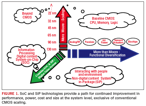
The electronics industry is nearing the limits of traditional CMOS
scaling. Although predictions that Moore’s Law has reached its limits
have been heard for years, they have proved premature. We are now,
however, nearing the basic physical limits to CMOS scaling, and the
price elastic growth of the industry can no longer continue based
solely on Moore’s Law scaling. New materials and device architectures
in development will eventually provide a path to increased density,
increased performance and lower cost beyond the capability of
CMOS-based circuits. However, there will be a time lapse between the
slowing of traditional CMOS scaling and the rollout of architectures
and materials that can support Moore’s Law scaling. In the meantime, as
scaling become more difficult, packaging innovations are taking up the
slack (Figure 1).

The
International Technology Roadmap for Semiconductors (ITRS) defines
functional diversification, incorporating system-level functions into a
single package, as “more than Moore.” This approach enables continued
rapid progress in functional density during a period where traditional
CMOS scaling cannot keep the pace and new architectures are not yet
ready. A second key contribution of packaging to maintaining the pace
of functional density scaling is 3-D integration. Both these
innovations are accomplished through integration of multiple circuit
types into a single device using system-on-chip (SoC) and
system-in-package (SiP) technologies. As electronics becomes more
consumer-dominated, the most important of these will be SiP. ITRS
defines SiP as “a combination of multiple active electronic components
of different functionality, assembled in a single unit that provides
multiple functions associated with a system or sub-system. SiPs may
optionally contain passives, MEMS, optical components and other
packages and devices.”
SiP technology enables the
efficient use of three dimensions through innovation in packaging and
interconnect. The result supports continued increased functional
density and decreased cost per function. Although there will be some
applications where SoC represents the better alternative, SiP provides
advantages over SoC in most market segments. The importance of these
advantages varies with different applications. They include:
- Small and custom form factors.
- Decreased weight.
- Reduced power consumption.
- High functional density.
- High frequency operation.
- Large memory capacity.
- High reliability.
- Low package cost.
- Lower development cost, greater integration flexibility, lower NRE cost and lower product cost compared to SoC.
- Rapid time to market.
- Wireless connectivity (GPS, Bluetooth, cellular, etc.).
SiP
is not a replacement for the high-level, single-chip, silicon
integration of SoC. It is complementary, and some complex SiP products
will contain SoC components. SiP technology is evolving from a
specialty used in a narrow set of applications, to a high-volume
technology with wide-ranging impact on electronics. The broadest
adoption of SiP to date has been for stacked memory/logic devices and
small modules used to integrate mixed-signal devices and passives. Both
these applications are driving high volume in very cost-competitive
markets. SiP has rapidly penetrated many market segments, including
consumer electronics, mobile devices, automotive controls and sensors,
computing, networking, communications and medical electronics. SiP’s
benefits vary by market segment but share some elements.
Time-to-market, size, power requirements and cost have resulted in
SiP’s strongest initial penetration: mobile communications. Unit
shipments have been rising at approximately 25% per year, and this
growth is forecast to continue.

Challenges for SiP
Traditional
single-chip packaging and system-level interconnect have limitations in
interconnect density, thermal management, bandwidth and signal
integrity that can be met only with new approaches. SiP technology is
the most important new technology to address these limitations.
Nonetheless, there are still a number of challenges, the most critical
of which are:
- Interconnection capable of maintaining power integrity for actives.
- Performance
and reliability of electronic systems are limited by the ability of
on-chip and off-chip system-level interconnections to maintain power
integrity during operation.
- Interconnect inductance,
high current requirements, increasing frequency and decreasing
operating voltage all increase the difficulty.
SiP
technology enables improvement in each of these parameters, but
challenges must be addressed if SiP is to meet its potential.
Thermal
dissipation. Inadequate thermal dissipation imposes the most serious
bottleneck to SiP performance. Not only does the thermal dissipation
technology dictate the chip junction temperature and subsequently its
performance, but the thermal technology’s size and cost will limit
packaging density, size and cost of SiP-based products. Thermal
dissipation is also the key limiter to 3-D stacking of microprocessors
and other high power/density ICs.
Signal bandwidth.
Even though bandwidth is often better than for single-chip packages,
inadequate chip I/O bandwidth is the third serious challenge to the
realization of ultimate performance. Losses resulting from package
substrate properties, crosstalk and impedance mismatches are
exacerbated as off-chip bandwidth per channel increases and signal
noise budgets decrease. Perhaps the greatest issue is the inability of
the small transistor to drive off chip impedance at high speed. SiP
technologies address these limitations and offer major improvements,
but much development work remains.
SiP Evolution
SiP
technology builds from the state-of-the-art in single-chip packaging,
with its advanced wirebond and flip-chip processes, by integrating new
technologies to support system-level integration. Emerging technologies
that will be combined with this base include wafer-level packaging, die
stacking, package stacking, through-silicon vias (TSV), 3-D packaging,
printable circuits, thinned wafers, and embedded actives and passives.
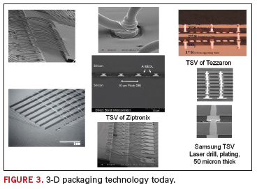
The current technical solutions for 3-D packaging include wire bonding,
face-to-face bonding and multilayer TSV structures (Figure 3).

Combining
these technologies into SiP devices provides a mechanism for
cost-effective functional diversification. These technologies enable
SiP to provide the necessary continuous increase in functional density
and decrease in cost per function. Market demands will result in the
integration of more components (e.g. passives, MEMS, optical and even
bio components) into a single package. The long-term vision for SiP is
the optimized heterogeneous integration of wireless, optical, fluidic,
bio elements/interfaces, as well as integrated shielding and heat
sinks. This goal requires new materials and control of their
interactions on the micrometer and nanometer scale.
Numerous
concepts for 3-D SiP packaging are emerging, driven largely by the
demands of portable consumer products. One of the most important is
wafer-level packaging. WLP is an emerging technology, used for both
single-chip packaging and SiP, where all elements of a package are
within the boundary of the die and all packaging processes performed
prior to wafer singulation into individual circuits. WLP development
was motivated by the recognition that WLP technology (i.e., parallel
processing on the wafer) addresses the need to increase performance and
functionality, while reducing system size, power and cost. WLP
technology with and without a redistribution layer (RDL) is used for a
variety of products where the small size, thickness and weight are
important product differentiators. This technology will provide
significant cost reductions as it matures and production volume
increases.
The combination of WLP and wafer/die
stacking approaches leads to a large number of variations in WLP
technology used for SiP. The highest levels of integration are achieved
through 3-D packaging. Die stacking has been used for consumer products
(such as cellphones) for several years, with wire bonding used to
connect the stacks to the package substrates. An important new
technology is through-silicon vias, which allow more efficient die
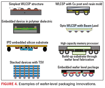
stacking and 3-D integration. These developments lead to more complex
packages for both single and multi-die WLPs (Figure 4).

The
use of TSV as a base for SiP requires solutions for both the thermal
density associated with a “cube” of transistors (rather than the planar
array of traditional CMOS) and the incorporation of passive devices
required for system-level integration. Prototypes have been developed
addressing both requirements. Microfluidic components with a form
factor suitable for lamination into a device stack with TSV
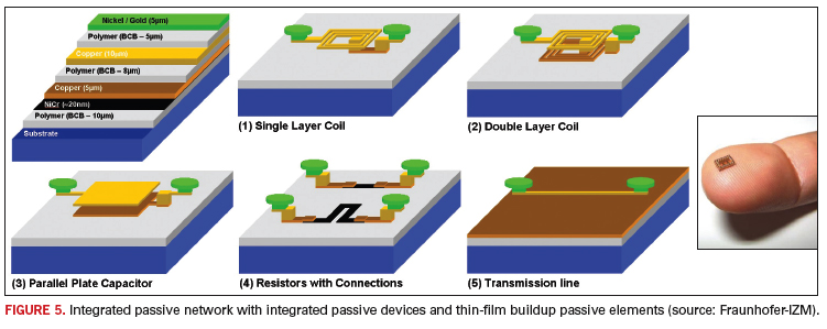
interconnect have been fabricated. Passive networks have also been
fabricated that are compatible with TSV interconnected die stacks (Figure 5).

Innovations
in SiP and WLP technologies depend on the integration of progress in
the integration of materials and equipment made in all segments of the
industry. The successful integration of all of these elements provides
a rich portfolio of capabilities in the era of “more Moore” (continued
CMOS scaling) and “more than Moore” (the addition of functional
diversification). Some of these advanced packaging elements include:
- New
materials such as nanoparticles to lower processing temperatures and
nanotubes for improved thermal and electrical conductivity.
- High-density, low-cost packaging substrates.
- Wafer thinning, singulation and handling.
- Embedded and integrated passives and actives.
- Co-design tools.
- Equipment for advanced packaging.
Innovations
in SiP have been accelerating, as this technology becomes a major
enabler for a large class of products in the consumer-driven
marketplace. Many issues remain that require continued research and
development. Today we have not proven the reliability of package-level
system integration for complex systems; we do not have a proven
strategy for repair and rework of SiP-based products; and we have not
resolved the test access and test contactor challenges associated with
the high frequency of future devices that will exceed 15 GT/s.
As
3-D SiP packaging architectures evolve, advanced co-design tools linked
with modeling and simulation capability must be in place to facilitate
an effective collaborative environment between system, device and
packaging engineers. New materials must be developed to meet the
requirements of these new SiP architectures and for meeting (changing)
environmental regulatory requirements. As an integrator of components
and technologies from different areas, SiP will become the primary
architecture for high-value, system-level products for consumer
products, before proliferating into products in all major market
segments. PCD&F
Dr. W.R. (Bill) Bottoms
is chairman and CEO of NanoNexus (nanonexus.com) and chairs the
Packaging Technology Working Group (TWG) for the iNEMI Roadmap and the
ITRS Roadmap for Assembly and Packaging; This email address is being protected from spambots. You need JavaScript enabled to view it..


