New paste materials and advances in screen-printing equipment create a flexible opportunity.
It has always been an industry vision to build electronic circuits
on a substrate by means of a simple printing process. It could be one
of the reasons why they were named printed circuit boards. This vision
has finally been realized by screen printing conductive pastes onto
flexible substrates.
In the early era, this
technology was applied only to low-technology circuits because screen
printing was a low-resolution process not capable of fine-line
circuitization, and there was a lower reliability in the material sets
used. Instead, the wet etching process with photolithography that uses
copper-clad laminate materials has been employed as the manufacturing
process of fine-line and complicated, patterned PCBs for the growing
electronics industry.
From its inception in the early
1950s, flexible printed circuit manufacturing has been an interactive
process changing to encompass new materials, equipment and the demands
of customers to package more functionality at a reduced cost. The first
applications were military aircraft and missiles where reliability,
reduced size and weight and the ability to conform to packaging
structures were of prime importance. These early applications were far
less dependent on meeting cost goals than the consumer electronics
market that predominates today’s flex usage. As the market has evolved,
so have the manufacturing processes to meet these changing demands.
Some of the earliest flexible printed circuits were made by screening a
conductive paste onto a dielectric base. However, reliability concerns
by the military led to the adoption of photolithography on copper-clad
substrates as the industry standard. In recent years, a re-emergence of
the printing process to mass produce electronic circuits has started to
gain favor, as the need to cut production costs continues to drive
technical advances in the interconnect industry. Various processes,
including printing etch resists on copper substrates to dot matrix
deposition and screen printing conductive materials on dielectric base
films, have been developed or refined. The circuit density capability
of volume production processing has always been the limiting factor.
Printable Electronics Materials
Recently,
researchers and engineers have been reevaluating the printing process
as a new electronic manufacturing process because of the capabilities
it offers that cannot be achieved by wet chemical and photolithographic
methods. A lot of new organic base materials have been developed as the
substrate for printable electronics in the last five years. Several
material companies have commercialized “nano paste” products that can
be used as conductive material to make fine traces. And yet, many
researchers have been developing new supplemental materials. They can
incorporate more functions than the simple copper foil conductors
etched by the photolithography process. They can incorporate the
characteristics of high-resistance materials, high-dielectric constant
materials, Piezo effect materials, semiconductor materials, electronic
luminescence materials and more.
These new
materials can be applied by a simple screen-printing processes to
create more electronic functions on the substrates. Currently, only
limited quantities of circuits with special constructions are in
commercial use at the high-volume production level. The reason is lower
resolution and a limited ability to manufacture multilayer circuits
compared to traditional photolithography processes. Specifically, no
basic printing process has been established for multilayer fine
flexible circuits with micro via-hole connections.
Advanced Screen-Printing Technologies
A
series of advanced screen-printing processes have been developed as the
basic manufacturing technology of “Printable Electronics” by DKN
Research and NY Industry. The new processes provide equivalent or more
capabilities to build complicated circuit constructions compared to
traditional subtractive process of copper foils or laminates with the
photolithography.
An optimized combination of the
process condition and material can generate 30 micron line/space on the
thin flexible substrates. Supplemental processes are capable of
generating 80 micron via holes for double-sided and multilayer
circuits.
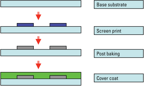
The basic flow of the advanced screen-printing processes is the same as the traditional screen-printing process as shown in Figure 1.
It is very simple. A paste material is printed on a thin flexible
substrate by screen printing and is baked. If necessary, supplemental
screen printing is conducted on the conductor traces. The key to this
advanced process is the optimized combination of the materials, screen
printers and screen masks. An optimized process condition generates 30
micron line/space on a thin but smooth substrate using nano-conductive
paste. Printing machines and screen masks are already capable of screen
printing 20 micron line/space. Industry is looking for capable
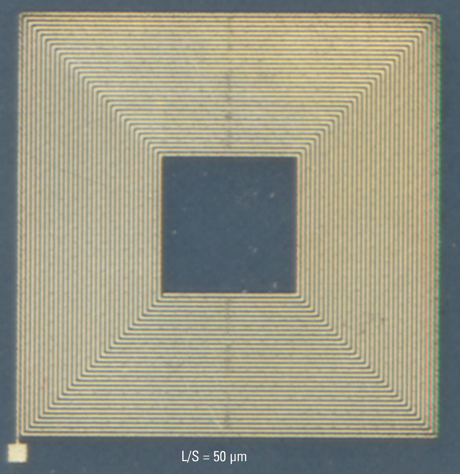
nano-conductive paste materials to realize the ultra-fine conductors. Figure 2 shows an example of a coiled circuit with a resolution of 50 micron line/space.
|

FIGURE 1. Basic process of screen printing.
|
|

FIGURE 2. Example of fine lines produced by screen printing.
|
Double and Multilayer Processes
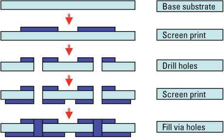
Multiple printing processes with appropriate via-hole technologies are able to produce double-sided and multilayer circuits. Figure 3
shows one of the via-hole generation processes for double-sided
circuits. First, a conductor paste is screen printed on a thin plastic
film as the first conductor layer. Second, small holes are drilled on
the conductor pads. The piercing machine with a CCD alignment system
minimizes the shifts to less than 50 microns. Third, the second
conductor layer is screen printed on the other side of the first
conductor layer. One more screen printing of the conductor paste is
conducted to make via-hole reliability higher.
|

FIGURE 3. Double-sided process with drilled via holes.
|
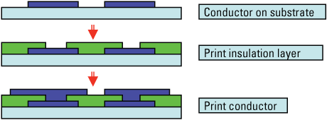
Figure 4 shows the buildup process of the advanced
screen printing to add more conductor layers on the basic constructions
of the flexible circuits. An insulation layer is screen printed on the
conductor layer with small access openings followed by another screen
printing of the conductor paste. The screen printer with a charge
couple device (CCD) alignment system minimizes the shifts between the
layers.
|

FIGURE 4. Build-up process with printed via holes.
|
Creating Additional Functionality
The advanced printing process creates more functions than copper
foil circuits produced by the traditional etching process. The printing
process is able to produce not only conductors on substrates but also
dielectrics, capacitors, resistors, coils, diodes, transistors,
electroluminescence devices and more as the embedded components in the
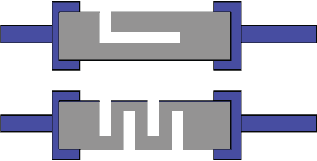
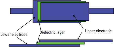
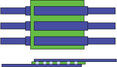
multilayer circuit. Some of the ideas are illustrated in Figures 5 and 6.
The resistor elements can be formed between two pads of the conductor
layer by screen printing a high-resistance material such as carbon
paste. High accuracies of the resistances were made by trimming carbon
patterns. The capacitance elements need a two-step screen-printing
process to generate the conductor layer. The capacitance materials with
high dielectric constants are screen printed between the two electrodes
that have been previously generated by a separate screen-printing step.
|

FIGURE 5. Screen-printed resistors followed by trimming.
|
|

FIGURE 6. Screen-printed capacitors.
|
Material Selections
Materials are the key to
good performance of the functional printed circuits made by advanced
screen-printing processes. Depending on the intended application, there
are a broad range of material choices for each function with printable
electronics. Each material has qualities that must be matched to meet
the requirements of the environment in which it will be used (Table 1 [PDF format]).
Following
material selection, the printing process is adjusted to meet the design
parameters of these materials and the requirements of the final
applications. Various types of screen masks are imaged by using the
customer’s Gerber data to form the circuit patterns, along with the
requisite positioning datum points, so that proper alignment can be
maintained. Ink selection is critical, matching conductive particulate
size and viscosity of the suspension medium. As the line width of the
circuit decreases, the particle size needs to be reduced, at times to
less than 3 microns, to minimize the chance that an open can occur
because of no conductivity between particles within a trace.
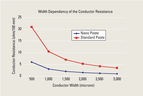
Figure 7 shows an example of the material
selections for the circuit design. The resistance of the conductors is
proportional to the length of the traces and inversely proportional to
the width and thickness of the traces. Substrate materials make few
contributions on the physical performances of the screen-printed
traces. Nano pastes shows about three times higher conductivity for the
traces compared to the traditional silver paste. Appropriate correction
factors should be provided for patterns finer than 100 micron traces.
The electrical performances are not proportional in these ranges. The
properties will need to be measured for each design.
|

FIGURE 7. Conductivities of the screen-printed traces. (Conductor thickness: 3 microns.)
|
Table 2 [PDF format] indicates the processing capabilities of the advanced screen printing to produce high-density, flexible circuits.
Combinations with Other Devices
The
technical capabilities of advanced screen printing are quite broad.
Flex fabricators can build many kinds of constructions for the
functional printed circuits without the help of other technologies.
However, appropriate combinations with other circuit technologies and
materials will generate more value.
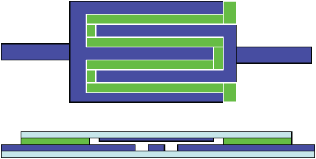
Figure 8 shows an example of the membrane switches.
A simple screen-printing process has been used that produces a large
volume of membrane switches for the keyboards of electronic products.
|

FIGURE 8. Switch construction made by screen printing.
|
Figure 9 shows ACP (anisotropic conductive paste)
termination of the flexible circuits with the other circuit devices. An
ACP material is screen printed on one side of the device. Then, two
devices are layered together with bond pile, and appropriate pressure
and heat are added to complete the connections. An optimized
combination of the ACP material and process condition is capable of
making reliable connections of the flexible circuits with 150 micron
pitches.
|

FIGURE 9. Interconnection of flexible circuits by screen-printable anisotropic conductive paste.
|
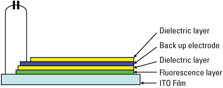
Figure 10 shows a unique idea of a lighting system
built on a thin, flexible substrate. All of the active and insulation
layers are formed on a transparent ITO (indium tin oxide) film by
screen printing. It is indicating a great possibility of large-size
flexible displays with low cost.
|

FIGURE 10. Electroluminecsence device built with a screen-printing process.
|
Applications
The combinations of these new
technologies will be valuable in producing new ideas for
next-generation electronics products such as switching modules, sensor
modules, bendable area light sources, thin flat speakers, flexible
displays, RF devices, small-size antennas, disposable medical devices
and more. New screen printable electronic materials will create more
application ideas in the future.
RTR (Roll to Roll) Capabilities
Most of the printing and piercing processes are technically ready to be
applied to RTR processes that have high productivity for the volume
productions. The use of high accuracy CCD alignment systems will
increase the overall process yields of multiple screen-printing
processes.
Conclusion
Screen
printing is not a new technology in the printed circuit industry.
However, the combination of new paste materials and the advanced
screen-printing process have created additional opportunities in
printable flexible electronics that cannot be made by the traditional
photolithography processes beginning with copper foil coated
substrates. More ideas will continue to be generated with these new
materials for specific applications. Multiple RTR processing will add
value to advanced screen printing by achieving low-cost manufacturing
for many flexible electronics components. PCD&F
Robert Turunen (This email address is being protected from spambots. You need JavaScript enabled to view it.) is vice president of new business development of DKN Research, Haverhill, Massachusetts. Masafumi Nakayama (This email address is being protected from spambots. You need JavaScript enabled to view it.) is president of NY Industry, Ohtsu, Japan. Dominique Numakura (This email address is being protected from spambots. You need JavaScript enabled to view it.) is managing director of DKN Research, Haverhill, Massachusetts.


