µPILR technology can reduce the standoff between the PCB and the
bottom package and increase mechanical board-level reliability,
improving drop-test performance.
The past decade has seen a tremendous market demand for driving more
and more functionality into applications in the mobile space. The cell
phone is a prime example of this trend as our daily communication,
computing and consumer electronics needs merge from discreet, handheld
units into one multifunctional device.
The basic cell
phone took off in the 1990s as a novelty with voice only. The
introduction of the color screen in 2000 and the camera module in 2002
were innovative developments that dramatically changed the way we view
our mobile devices. Several other applications have been integrated,
and today, our cell phones offer advanced functions such as digital TV,
GPS, MP3 technology and more security as we search the web, enabling
our on-the-go lifestyles. The integration and miniaturization of all
components within the device has become a necessity to achieve the
reduced form factor and weight demanded by consumers.
The
silicon stacking industry has seen many revolutions, with memory
stacking for a memory subsystem to system-in-package (SiP) with the
inclusion of logic devices. Die stacking logic and memory was a quick
way of initially achieving the desired form factor, but the cost was
not sustainable long term due to the compound yield loss of the total
package. In 2005, the introduction of package-on-package (PoP) into the
industry allowed the logic and memory sub-system packages to be tested
separately and reduce the cost. Figure 1 shows an
illustration of the production PoP in mobile phones today. PoP
technologies have become a main standard for these applications,
allowing designers to match technological advancements in functionality
with increasingly smaller form factors. This article will discuss two
main approaches for miniaturizing PoP via finer pitch: memory
sub-system package stacked on package with one logic die or two logic
die.
|

FIGURE 1. Illustration of the production PoP in mobile phones today.
|
Market Trends for Package-on-Package
The
current industry standard for the PoP inter-package ball-out interface
is at 0.65-mm ball pitch, and package sizes range from 11 mm x 11 mm to
16 mm x 16 mm with varying architectures. The bottom package (for the
processor) is 0.5-mm pitch with a custom ball-out based on the
processors.
Tessera recently conducted a study to
evaluate pitch trends for the logic IC in mobile applications from 2003
to 2007. The study examined 110 mobile phone teardowns from
Portelligent (portelligent.com). In 2003, approximately 30% of these
ICs were at 0.5-mm pitch, and the rest ranged up to 0.8-mm pitch.
Today, over 98% of these logic ICs are now at 0.5-mm pitch.
The
increasing number of applications in mobile devices and subsequent
higher performance demands require higher pin counts, which typically
increases size. This requires the footprint to remain the same or
become smaller. Accommodating these higher pin counts in such a
footprint will require smaller pitch. There are several ways the
industry is reducing or maintaining the overall footprint. This article
will discuss two main approaches when dealing with PoP stacking.
The
first option is to reduce the solder ball pitch, which reduces the
packages X-Y size. Logic IC packages are trending toward 0.4-mm pitch,
driving the top memory sub-system package to reduce from the current
0.65 mm to 0.5-mm pitch. This option will achieve a smaller package
size of the one component as its performance increases from one
generation to the next.
The second option allows
for higher integration while maintaining or reducing the solder ball
pitch and, in return, reducing the overall footprint of two or more
packages into one. Stacking a second logic IC into the bottom package
will increase the package size for the PoP but will reduce the overall
combined size of the two separate packages (one stand-alone logic
package and one PoP). This option will also increase the I/O count, and
the package can remain at 0.5-mm pitch to maintain good routing or
reduce to 0.4-mm pitch for size benefits. In either case, the top
memory sub-system package can remain at 0.65-mm pitch to maintain the
memory interface I/O count for the larger package.
PoP Challenges with New Market Trends
These
two PoP approaches will enable increased integration and reduced
overall form factor to allow for continued increases in performance and
applications in mobile devices. However, both options have their
challenges.
For the first option, the reduced pitch
on the top package will result in smaller clearance between the two
packages. A logic die can be connected to its substrate via wire bond
or flip chip. Currently, the clearance between two packages using
either interconnection method for 0.65-mm pitch is approximately 0.270
mm to 0.320 mm. When the top package pitch is reduced to 0.5 mm, the
clearance will reduce to approximately 0.220 mm due to the smaller
solder ball used for this smaller pitch. In turn, this will require
reduced height in the logic IC. Reducing the height for wire-bonded die
would mean die thinning to ≤75 µm and/or reducing the wire bond loop
height. Reducing flip-chip height will also require die thinning and/or
reduce the bump height. There is also a cost premium associated with
lower wire-bond loop heights, and reduced mechanical reliability for
lower bump heights for flip chips. All these solutions increase
performance risk and cost due to die thinning and handling.
The
second option – stacking two logic die in the bottom package – will
require an increased clearance between the two packages. Increasing
solder ball size to achieve this increased clearance will require
higher pitch for the memory sub-system to avoid solder bridging. In
addition, the higher pitch will reduce the I/O count for the
package-to-package interface if the same X-Y size is to be maintained.
These
challenges are difficult to overcome within the current technology
window while maintaining the cost and risk targets. The industry is
examining innovative new approaches to take packaging technology to the
next level. One new option is the Micro Pin Interconnect Layer (µPILR)
technology developed by Tessera, which addresses many of these
challenges.
µPILR Technology for PoP
The
µPILR technology platform utilizes conical-shaped, solid copper
contacts plated with nickel/copper. This can be used in multiple types
of interconnections:
1. IC-to-package substrate interconnections
2. Package-to-PCB and/or PoP interconnections
3. Interlayer via connections within package substrates, flexible printed circuits or high-density PCBs.
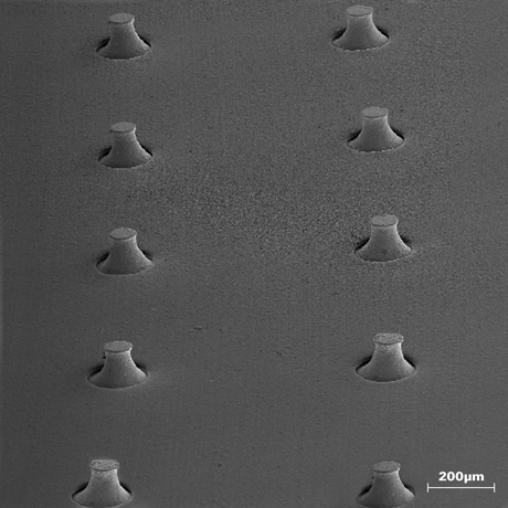
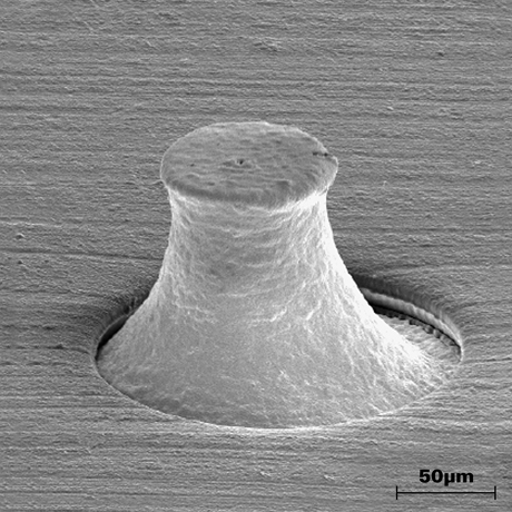
Figures 2a and 2b
show SEM images of this contact. This article will mainly discuss the
package-to-package and PCB-to-package interconnections for PoP.
|

FIGURE 2a. SEM image of a µPILRTM contact (125 µm height with 80 µm tip).
|
|

FIGURE 2b. SEM image (higher magnification) of a µPILR contact (125 µm height with 80 µm tip).
|
The
introduction of the solid copper contact within a solder joint provides
better ability to control and hold standoff while maintaining solder
interconnect reliability at the board and package-to-package level of
the PoP.
This technology can reduce the standoff
between the PCB and the bottom package by more than 50% to allow
overall package height reduction. Due to the increased surface area
between the copper and solder when using µPILR, there is an increase in
mechanical board-level reliability, especially drop test. Figure 3
illustrates initial drop test data where the addition of the copper pin
shows late first failures using JESD22-B111 drop test conditions. The
test vehicle for the data was on a 10 mm x 10 mm package size with the
full area populated with µPILR contacts. The drop test was performed on
this test vehicle with multiple pitches – 0.65 mm, 0.5 mm and 0.4 mm –
using 196, 324 and 529 total µPILR contacts, respectively. To simulate
an actual device, the silicon size used was 6.5 mm x 6.5 mm x 150 µm.
This was attached to the top surface of the substrate using paste die
attached material. The overmold height for the package was 450 µm over
the substrate.
|

FIGURE 3. Drop test data using µPILR showing first failures for 0.4 mm, 0.5 mm and 0.65 mm pitch.
|
A theoretical stack-up analysis of the test vehicle (shown in Figure 4)
using the tolerance stacking methodology shows that less than 1.2 mm
total height can be achieved. The test vehicle consists of one die in a
bottom package at 0.4-mm pitch, three die in the top package at 0.5-mm
pitch µPILR and a two-layer µPILR substrate (top and bottom).
The
ability of µPILR to control standoff at the package-to-package
interconnect level allows for higher clearance between the two packages
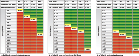
while maintaining the needed finer pitch. Figure 5
(left and middle side) shows the difference between the resulting
standoffs for solder ball and µPILR PoP, respectively, at the
package-to-package interface using the same solder ball diameter and
pad opening. Figure 5 (right side) also shows the resulting standoff
with a smaller solder ball and pad opening.
|

FIGURE 4. Test Vehicle for µPILR PoP with one logic and three memory die at <1.2 mm total package height.
|
|

FIGURE 5. Inter-package stand-off of PoP using solder balls only versus µPILR with solder. Inclusion of µPILR increases joint stand-off.
|
This
data was calculated using an in-house developed software utility. This
software calculates the resulting shape of the solder (diameter and
height) based on the initial volume of solder. The final shape can be
calculated for different cases including solder reflowed on a pad,
solder ball reflowed to make the joint between two packages, or between
package and PCB. The calculations are based on the assumption that the
surface tension dominates, and hence, the free solder surface is
spherical. If the package weight per interconnect ratio is high enough,
then gravity will have a significant effect, which is not accounted for
in this tool. For standard packages, package weight/interconnect ratio
is small enough that the results from this tool are quite accurate when
compared to actual observed data.
To meet market
demands for a smaller 0.5-mm pitch at the package-to-package interface
and to keep the risk factor on the logic device as low as possible, the
desired stand-off would need to remain at approximately 0.270 mm.
Figure 5 (left side) shows that a solder ball-only solution cannot meet
this requirement unless the solder ball size is increased, which
increases the risk of solder bridging. Using µPILR, Figure 5 (middle),
allows better control of the standoff to achieve the desired clearance
by forming a column-like structure. Since µPILR can provide improved
joint reliability, the same calculation was done with a smaller pad
opening, as shown in Figure 5 on the right side. This allows for a
higher margin for the standoff. The standoff for the contact using
µPILR can be further increased by increasing the total solder volume.
Surface-mount
experiments showed that increased solder content enables a higher
standoff at the same finer pitch without bridging, mainly because µPILR
causes the joint to form a column-like structure, which is more robust
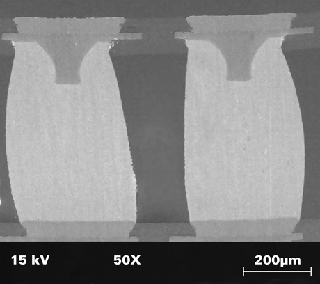
than a solder-only joint. Figure 6 shows a SEM
picture of a 0.125-mm µPILR copper pin surrounded by solder to form an
interconnect with a standoff of 0.540 mm. A clearance this high also
facilitates the second approach of stacking two logic ICs in the bottom
package of a PoP as mentioned earlier.
|

FIGURE 6. SEM picture of a 0.125 mm µPILR copper pin surrounded by solder to form and interconnect with a stand-off of 0.540 mm.
|
As
the industry continues the trend toward tighter integration in mobile
devices, stacking two logic devices in the bottom package for PoP will
allow for higher performance and smaller overall form factor. However,
this results in a thicker mold cap height on the bottom package, which
requires a larger standoff clearance between the two packages. At even
larger pitches such as 0.65 mm, solder ball interconnect cannot
overcome this mold cap height. However, by applying the concept of
increased standoff ability with the µPILR technology to this
application at 0.65-mm pitch, designers will be able to realize more
integration between the logic and memory.
Testing
will be conducted on daisy-chain test vehicles, board-level reliability
on the µPILR PoP test vehicle with one die as shown in Figure 4 at 0.5
mm, and with two die at 0.65-mm pitch in the bottom package and up to
three die in the top packages. The data will be available in late 2007
and early 2008, respectively. The test vehicle will be RoHS compliant
with a halogen-free material set. Testing will cover JEDEC JESD22-B111
for drop (1500 gn, 0.5 ms pulse, 30 drops), JEDEC JESD22-A104 Condition
G for temperature cycling (-40ËšC to +125ËšC until 63% fail, 10 minute
dwell, 10ËšC/minute ramp rate; continuous monitoring of resistance) and
JEDEC-9702 for monotonic bend test (4-Point Bend; 5000 µStrain/s).
Package
assembly with µPILR technology uses standard semiconductor assembly
equipment for all major processes, including die placement, wire
bonding and overmold. The surface-mount technology required for µPILR
is dependent on the resulting standoff needs, since the copper pins are
coated with nickel and immersion gold to allow for high-strength
adhesion of solder. If the interconnect standoff is to be minimized for
height reduction between the bottom package and PCB, for example, then
the ball attach process at package assembly can be eliminated, and the
surface mount can be performed by optimizing the solder paste content
on the PCB. The µPILR package can then be picked, placed and reflowed
in the same manner as any other component. For higher standoff
requirements, such as between packages, solder can be pre-applied to
the µPILR copper pins. Additional solder paste or solder balls can be
placed to the pad opening on the top interface of the bottom package.
The total solder content can be optimized to achieve the required
standoff for the clearance needed. Thus, surface-mount assembly can
utilize existing processes, materials and equipment without incurring
additional capital expenses.
Conclusion
Looking
ahead, logic IC packaging will reduce interconnect pitch from the
current 0.5 mm to 0.4 mm, driving technology capability toward higher
I/Os and/or smaller packages. The smaller overall package size results
in a lower I/O count for the memory interface at the current 0.65-mm
pitch. Driving the memory module to 0.5-mm pitch will either maintain
or increase the I/O count. However, 0.5-mm pitch standoff between the
logic and memory interface will increase the risks and costs with the
need to reduce thickness within the logic arena.
Technologies
of this type are being introduced to the market to allow for finer
pitch with the ability to control solder standoff, while using existing
assembly and surface-mount infrastructures. As these technologies
mature and gain broader adoption, they will serve as the catalyst to
enable future innovation in the converging mobile devices market. PCD&F
Ed. – In a follow up to this article, Printed Circuit Design & Fab will publish the data generated from the daisy-chain, board-level reliability testing when it becomes available.
Manisha Sharma is senior product marketing manager, Tessera Inc. She can be reached at This email address is being protected from spambots. You need JavaScript enabled to view it..


