OEM designers and their EMS partners should evaluate SerDes device characteristics and match them to known PCB design constraints to improve overall performance.
Serializer/deserializer (SerDes) technology is pushing parallel-based architectures out of the way and rapidly becoming an integral part of high-speed PCB designs. Many designers are learning that SerDes device specifications vary and are difficult to fully grasp since the technology is still relatively new. In these instances, a savvy EMS provider experienced in these designs can help prevent erroneous SerDes selections.
At last count, there are over 20 SerDes device vendors, each with their own flavors. Therefore, it is up to OEM designers and their partner EMS provider to carefully inventory the design and application strengths and weaknesses of these various SerDes devices. This includes careful evaluation of their unique characteristics, speed, noise immunity and jitter levels, among other considerations. SerDes significantly contributes to system frequency and device pin density, thus PCB layout becomes more complex. These design factors can prevent fully optimized SerDes performance if the wrong device is used.
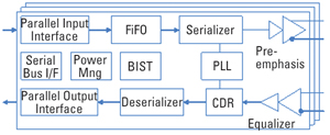
As shown in Figure 1, SerDes can be an intellectural property (IP) core in a complex ASIC, FPGA, ASSP or IC with all the SerDes functions integrated in it. In effect, a SerDes is a transceiver that converts parallel to serial data and vice-versa. The transmitter section is a serial-to-parallel converter, and the receiver section is a parallel-to-serial converter.
|

FIGURE 1. Example of a SerDes I/O IP core. (Courtesy of IPtronics A-S)
|
The serializer takes 8-bit parallel data input, converts it to 10-bit, and then transmits it over a serial output link. The deserializer performs the reverse process by decoding serial data and converting it to parallel format. Multiple SerDes interfaces are often housed in a single package.
SerDes facilitates the transmission of parallel data between two points over serial streams, reducing the number of data paths and thus the number of connecting pins or wires required. Most SerDes devices are capable of full-duplex operation, meaning that data conversion can take place in both directions simultaneously. SerDes are used in gigabit Ethernet systems, wireless network routers, fiber optic communications systems and storage applications. Specifications and speeds vary depending on the needs of the user and on the application. Some SerDes devices are capable of operating at speeds in excess of 10 gigabits per second (Gbps).
SerDes Has Many Facets
There are countless facets to deal with when selecting the right SerDes for a given high-speed PCB application. However, the top ones include programmability vs. non-programmability, latency and key parameters, and characteristics such as output drive and phase-lock loop variations.
There are two types of SerDes devices; one is a programmable SerDes block in an application specific standard product (ASSP) IC and the other is non-programmable. The programmable version offers several advantages to the OEM designer. Due to its re-programmability and flexibility, it allows a PCB to be more customizable so that the designer can use any local bus (either PCI or proprietary). As a result, component costs are reduced and time to market is shortened. Programmable SerDes also permits flexible IO assignments. This enables the designer to select optimal pin assignments, thus easing board layout and reducing layer count. Plus, programmable SerDes provides I/O voltage level and I/O type programmability.
Latency issues are most prominent in backplane technology, which uses SerDes extensively. Large shared memory accessed by multiple cards is used to reduce the PCB area. Sometimes designers implement the backplane connection in a parallel configuration while developing a multi-processor shared memory system. Thus, the resulting number of traces routed across a backplane becomes a major consideration.
Most often, designers are tempted to use the highest speeds possible when implementing a high-speed SerDes design, for example, greater than 2.5 Gbps. In this case, the SerDes receive side always has greater latency than the transmit side due to decoder and buffering requirements. The latency is usually between 130 to 150 ns on the receive side and 70 to 90 ns on the transmit side.
The amount of latency becomes unacceptable if a large FPGA is used to integrate the SerDes block. A better option is a SerDes with a limited amount of programmability, specifically one that only programs I/Os and voltage levels. This limited programmability and lower latency translates into high speeds with less component and routing densities.
The trade-off is low programmability. A denser SerDes should be used in applications such as PCI bus interface that require flexibility and more programmability. Here, an FPGA can help combine the PCI interface with SerDes, but increases latency by as much as 40%.
Check Out Parameters
There are a number of parameters to investigate while selecting the right SerDes. However, the most important ones are receive jitter (RX) tolerance, transmit jitter (TX), the eye diagram and power consumption.
All signals have some amount of jitter. Some are deterministic, which relates to repetitive events, while others are random jitter. RX jitter, measured in UI or unit interval, occurs on the receive signal. It is important for a design engineer to understand the level of jitter tolerance a SerDes has and how appropriate it is to a given application. RX jitter tolerances vary from one SerDes vendor to another. While a considerable amount of jitter can be controlled at PCB layout, an engineer’s goal should be to select a SerDes device that is more tolerant to jitter at the frequency the device needs to operate.
It’s important to note that many SerDes specifications omit any reference to frequency-dependent jitter. Usually deterministic jitter increases with frequency. Moreover, the effects of clock jitter are often neglected, which can cause detrimental effects on overall device jitter tolerance.
TX jitter, measured in UI or unit interval, is created by the SerDes device and is reflected on the transmitting side of the serial link. Ideally the SerDes device should be able to transmit a signal with minimal jitter. In this case the lower value of UI is better.
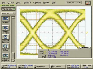
As shown in Figure 2, an eye diagram is a graphical representation of how cleanly the data is transmitted by the SerDes device (signal integrity). The eye shows amplitude and time period or the amount of time the eye is open expressed as UI.
|

FIGURE 2. Example of an eye diagram over 20" FR4 at 3.7 Gbps.
|
Power consumption is critical because a more complex SerDes device draws considerable power and dissipates a considerable amount of heat. It is not uncommon to find a SerDes block integrated in an FPGA that requires as much as 500 million W. Again, the designer is faced with tradeoffs. Either they need to use a densely packed, highly programmable SerDes device that draws inordinate power, or they opt for a simpler, low programmable device that has less wattage requirements and is less flexible. Hence this trade-off factor, like latency, is also application specific.
Output Drive and PLL
Aside from these key SerDes considerations, there are two particularly important SerDes technical characteristics that can vary among vendors: output drive and phase-lock loop (PLL). It is vital for OEM designers to understand them and how they can affect a high-speed PCB design.
Low-voltage differential signaling (LVDS) is used for SerDes devices as the most common drive. LVDS cuts down on noise, known as common-mode noise rejection, and boosts data rates by using extremely low voltage levels, translating to low radiation and less power consumption.
Most important, differential signaling allows the receiver to filter out noise. This is done by simultaneously sending signals across two wires, each with opposing current and voltage swings. Actual data is read as the difference in amplitude between the signals on the two wires. If noise is induced, it will appear on both lines but the signal information remains unchanged. Since the signal has improved noise immunity, voltage can be reduced and data rate can be increased.
Some SerDes devices have higher speeds and drive. In these instances the IC vendors substitute LVDS with emitter-coupled logic (ECL). This type of SerDes is best for driving a cable longer than 15 meters at high speeds. ECL-based SerDes usually provide designers with speeds of 2 GHz, while LVDS provides 600 MHz speed. The design trade-off related to ECL SerDes is extremely high power consumption; six times greater than that of LVDS. As a result, ECL-based SerDes is directed at highly specialized applications. This type of SerDes is overkill in applications calling for low power consumption.
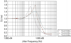
PLL is used to keep time for the differential pairs of the SerDes in each device. The best way to compare PLLs of each vendor is to do a jitter bandwidth test because the PLL operation is critical to the working of a SerDes. Figure 3 shows sinusoidal jitter being injected into three devices at same carrier frequency. The general trend shown by the graph is that output jitter from the PLL increases gradually with the frequency of the jitter. The graph shows that the device that has lowest peak and bandwidth outputs the lowest jitter.
|

FIGURE 3. Serializer jitter transfer function.
|
The PLL block within the SerDes receives a system reference clock and multiplies it to an appropriate data rate. A separate sampler block uses the resulting clock to latch incoming serial data. Therefore, as the name implies, the phase-lock loop’s job is to lock to the input clock frequency, perform a correct multiplication factor and maintain its output with minimal jitter.
PLL operations may seem simple at first glance, but there is much detail. Time to lock, power consumption, loop correction factor resolution and jitter effects are the top layer of these aspects OEM designers must understand. OEM designers should use a jitter-bandwidth test as a way to determine the most effective PLL comparisons. Testing is often costly but the results are beneficial in selecting the correct vendor. PCD&M
Syed W. Ali is a certified interconnect designer and layout engineer, Nexlogic Technologies Inc. He can be reached at This email address is being protected from spambots. You need JavaScript enabled to view it..


