Bit rate and interconnect length influence lossy line effects.
With the start of the new year, I am giving my column a new name and look. Starting with this issue, it will have a question and answer format and be called The Signal Doctor.
Since presenting four Webinars*, eight keynote lectures and 10 classes last year I have been inundated with all kinds of questions. I thought it would prove helpful to share some of my answers with the design community.
Here we go with the first question from Brad of Syracuse, NY: What is a back-drilled via?
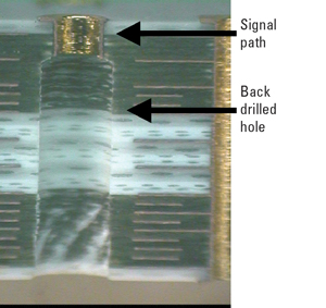
Answer: A back-drilled via is a normal through-hole via in a PCB that connects two signal layers, but the dangling stub hanging down from the last signal layer to the bottom of the board has literally been drilled out. A drill bit with a diameter a few mils larger than the drilled and plated hole drills out the stub. This removes the copper stub and prevents a potentially disastrous resonance in the 5 to 10 GHz range. All high-performance backplanes use back-drilled vias. Figure 1 shows an example of the cross section of a back drilled via in a thick backplane.
|

FIGURE 1. Example of the cross section of a back drilled via in a thick backplane.
|
Question from Jeremy in San Jose: When do I have to worry about losses in a transmission line?
Answer: The problem created by lossy transmission lines is the rise time degradation of transmitted signals due to frequency dependent losses from the conductors and the dielectrics. The rise time degradation contributed by the interconnect is only an issue when the bit period, or unit interval, of the signal is comparable to or shorter than the increased rise time. If the bit period is long compared to the rise time, the signal will have plenty of time to reach its full value in a bit period and the rise time degradation will have no impact on the signal quality.
For example, a signal with a bit rate of 2.5 Gbps has a bit period of 1/2.5 Gbps = 0.4 nsec. If the rise time of the signal is shorter than about half of this or 0.2 nsec, one rise time to get up and one fall time to get down, the received signal quality will not be affected much by the interconnect.
However, if the rise time, limited by the interconnect, were to increase to 0.2 nsec or longer, the pattern of the received signal would be affected by the interconnect. The voltage of one bit received would depend on the previous pattern. This effect is called inter-symbol interference (ISI) and gives rise to collapse of the eye diagram and deterministic jitter.
As a rough rule of thumb in FR-4, the rise time degradation is about 10 psec/inch of travel length, due to just the dielectric loss. A signal starting out with a 1-psec rise time will have a rise time of about 100 psec after traveling 10 inches. Lossy effects are important when the interconnect limited rise time is longer than half a bit period, or RT > 0.5 x 1/BR, with RT being the interconnect limited rise time, or 10 psec/inch x length, with BR as the signal bit rate.
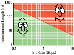
Using this rule of thumb, we see the relationship between the interconnect length and bit rate, when we need to worry about lossy lines as: length > 50/BR, with BR in Gbps and length in inches.
For example, if the bit rate is 2.5 Gbps, any line longer than 50/2.5 = 20 inches may have problems with ISI, collapse of the eye diagram and deterministic jitter. It doesn’t mean the interconnect won’t work, it just means that if you don’t run a simulation you may be surprised by product that doesn’t work. Knowing of a problem beforehand might give you an opportunity to design it right the first time, perhaps using a wider line, a shorter length, a lower dissipation factor laminate, routing on a surface microstrip, or a silicon processing technique such as TX or RX equalization.
|

FIGURE 2. Graphical representation of the rule of thumb that we must worry about lossy lines if the length of an interconnect is longer than 50/BR.
|
Figure 2 is a handy graph of this rule of thumb. If your combination of bit rate and interconnect length lands you above the line, in the red zone, you better worry about lossy line effects.
If you have a signal integrity related question you’d like me to address, send it to signaldoctor[at]upmediagroup.com and I will consider including it. I will only list your first name and your city. PCD&M
*Links to the archived versions are posted at BeTheSignal.com.
Dr. Eric Bogatin is president of Bogatin Enterprises. He can be reached at signaldoctor[at]upmediagroup.com.


