Enabling wickedly compelling mobile devices with greater functionality and elegant form factors.
The first was as thick as a brick ... The next is as thin as a razor,” was the advertising slogan used for the market introduction of the RAZR phone. Less than 20 years ago the mobile phone was a large, expensive, single-purpose device with few subscribers and limited coverage. Today it’s a small, affordable device available with a wealth of features and options that provides a convenient means for people to communicate. The functionality packed within the mobile device is growing while the device itself is getting slimmer, smaller, and easier to carry and use.
The future is in smaller, faster, thinner and affordable devices that provide the ability to connect anywhere, anytime, with any service to get uninterrupted access to information, entertainment, communication, monitoring and control. From the user’s perspective, that’s a pretty exciting future. But for device manufacturers, getting to that future quickly and competitively requires solving some daunting technology challenges. How does Motorola manage to include all of this technology while still creating iconic designs at affordable prices? Microminiaturization is the answer to making smaller and smaller devices do bigger and bigger things.
The Opportunities: A Closer Look
Miniaturization is not a new challenge for the electronics industry, and the industry has already demonstrated its ability to address the challenge in consumer electronics, communication and computing devices. While miniaturization of individual components and functions making up the handheld device is important, system-level microminiaturization of the handheld device is necessary to achieve the new functionality, design, performance and cost targets expected by the consumer. In addition to the traditional microminiaturization opportunities using silicon integrated circuits, to make real progress manufacturers also need to look at system architecture, product design, and electrical and mechanical components that haven’t received much attention in the past.
Identifying and exploiting these opportunities is only half of the solution. Success in the marketplace demands that microminiaturization technologies be designed and built into first-to-market products that can be shipped in very high volumes. This requires end-to-end coordination from technology development to product design and manufacturing, and requires a clear vision, sound technology planning, strong supply chain partnerships and flawless execution.
Due to the complexity of today’s product, ad hoc addition of functionality no longer works and a system level optimization of the product is essential. Let’s take a look at one of the more promising techniques.
Printed Circuit Board Integration: mesoMEMS
One often-overlooked opportunity for microminiaturization is integration of components inside the printed circuit board. The PCB is the core building block of all electronic devices, and provides an excellent platform for integration of passive electrical components such as resistors, capacitors and inductors, and electronic functions such as filters, baluns, dividers and couplers. Researchers at Motorola Labs have developed and implemented in mobile phones industry-leading technologies for embedding resistors, capacitors and inductors within the PCB. More recently, Motorola Labs has also demonstrated mesoMEMS capability. This is the ability to integrate electro-statically actuated movable structures to form high performance RF switches and tuning elements integrated with the PCB.
Motorola’s mesoMEMS technology is yet another advance in PCB level integration. While MEMS (Micro-electro-mechanical systems) are typically associated with silicon level fabrication, Motorola has developed the structures and processes required to fabricate a MEMS structures in the PCB. The term mesoMEMS has been coined to distinguish the scale of the MEMS structures fabricated in the PCB with those fabricated in silicon. mesoMEMS structures are in the order of hundreds of mils compared with typical silicon MEMS structures that are in the order of tens of microns.
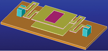
mesoMEMS structures can be used to “steer” electrons, leading to interesting RF applications (Figure 1). Motorola has demonstrated Single Pole-Single Throw (SPST) to Single Pole-Multi-Throw (SPMT) RF switches with excelleznt broadband performance using mesoMEMS technology. The switches are electro-statically actuated with actuation voltages and switching times being comparable to those reported for silicon MEMS RF switches. The RF power handling capability of the mesoMEMs switches, however, is far superior to their silicon MEMS counterparts.
|

FIGURE 1. Diagram of mesoMEMS structure for RF switching applications.
|
mesoMEMS RF switches are fabricated using PCB processing techniques. The costs, therefore, are significantly lower than their silicon MEMS equivalents that additionally require expensive hermetic sealing of the switch packages. Since Motorola’s embedded passives and mesoMEMS technologies are both based on PCB fabrication processes, both technologies can be co-fabricated in the PCB resulting in high levels of system-level microminiaturization, performance improvement and function integration. The excellent RF performance of the meosMEMs switches and tuning structures formed using the technology can be used to design tunable antennas and front-ends for complex multi-band/multi-mode mobile phones.
A mobile phone that incorporates different communications bands, along with WiFi connectivity, Bluetooth, satellite radio, mobile TV and other RF features, might need seven or more antennas. But micro-miniaturization technologies can be used to consolidate these antennas into a switchable multiband antenna – minimizing the space taken up by one of the larger components in any wireless handheld device. Motorola’s mesoMEMS technology can provide the RF switching needed to enable this antenna consolidation. By using mesoMEMS tuning and switching it becomes possible to make a smaller antenna that actually does the work of multiple, larger antennas.
Motorola is Leading the Way
For newly invented technologies to be commercially successful, one has to be able to manufacture devices using the technologies in high volume and in generating them with high yields. Once Motorola Labs develops a novel technology it also establishes the manufacturing supply chains needed through technology licensing. Motorola’s microminiaturization research provides the industry with design ideas, enabling technologies and fabrication methods that speed iconic designs to market. PCD&M
Aroon Tungare is director, Short Range Communications & Microminiaturization Technologies at Motorola Labs. He can be reached at This email address is being protected from spambots. You need JavaScript enabled to view it..


