Understanding reflections caused by transmission line characteristic impedance and termination impedance mismatch.
Analysis of “digital interconnects” is the analog problem in frequency domain where interconnects are simulated as transmission lines defined by characteristic impedance and propagation constant. Digital signals in interconnects are sequences of amplitude-modulated pulses that transmit bits between components. The “digital interconnect” analysis problem is technically an analog problem of pulse propagation modeling in time-domain.
The sequence of the transmitted bits (1s and 0s) is the only boundary between the digital and the analog interconnect analysis domains. That time-domain analysis problem, however, is practically always solved in the frequency domain. The pulse or sequence of pulses are transformed into a superposition of harmonics or sinusoidal signals in the time domain (more on that in Shlepnev1) because it is mathematically easier and more convenient to model all types of signal degradation for the harmonic signals using phasors and complex analysis. Components on PCBs in the digital domain are just connected – 1s and 0s are supposed to flow seamlessly among the components. In the analog or RF/microwave domain, components on PCBs or in a package are connected with the distributed open waveguiding structures composed of traces and reference conductors and simulated mostly as transmission lines. To ensure the digital signal gets through, we build interconnect models that include all signal degradation factors important for a specific data rate.
In general, all signal degradation factors can be separated into three categories:
• Absorption losses in dielectrics and conductors
• Reflection losses due to impedance mismatch and discontinuities
• Coupling losses and distortion (includes crosstalk).
Absorption or dissipation losses in dielectrics and conductors were recently discussed in Shlepnev2. Such losses are inevitable, but can be effectively mitigated at the stackup planning stage – selection of dielectric and conductor materials and stackup geometry defines the maximal possible communication distance for a particular data rate.
Considering the reflections, they can be further separated into the following categories:
• Reflections from transmission lines and termination impedance mismatch
• Reflections from single discontinuities – vias, transitions, AC caps, gaps in reference plane, etc.
• Reflections from periodic discontinuities – cut outs, fiber-weave effect, etc.
Why do we care about the reflections? Because the reflections degrade the transmitted signal, and such degradation may cause link failure. Thus, understanding and evaluating reflections is useful for channel quality control, and there are corresponding compliance metrics in the frequency domain (bounds on reflection loss) as well as in the time domain (effective return loss, or ERL).
Here we take a closer look at the reflections caused by the transmission line characteristic impedance and termination impedance mismatch. We discussed it in our “Design Insights…” tutorial at DesignCon in 20203 and this article is loosely based on that.
Impedance and admittance, as well as impedivity, admittivity, conductance (conductivity?), succeptance, leakance, voltivity, and gaussivity are the terms introduced by Oliver Heaviside at the end of the 19th century during the golden era of electromagnetic discoveries started by James Clerk Maxwell. Heaviside derived the telegrapher’s equations describing transmission lines or, as we know now, any waveguiding system in general. The equations describe a one-dimensional distributed problem that for a two-conductor or one-mode (one signal and one reference conductor) transmission line looks as follows:
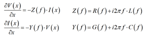
Eq. 1
Where I is the current, V is voltage changing along the x-axis, f is frequency [Hz], Z [ohm/m] is complex impedance per unit length and Y [S/m] is complex admittance per unit length, R [ohm/m] and L [Hn/m] are real frequency-dependent resistance and inductance per unit length, and G [S/m] and C [F/m] are real frequency-dependent conductance and capacitance per unit length.
Z, Y, R, L, G, C for N+1 conductor problem or N-mode transmission line are NxN matrices in general. They are 2x2 matrices for a three-conductor differential line for instance. The impedance and admittance per unit length are frequency-dependent in general and are completely defined by transmission line type and cross-section and usually computed either with a static or quasi-static 2-D field solver or sometime with 3-D EM solvers. Note the use of 3-D solvers does not automatically guarantee higher accuracy.
A solution of the telegrapher’s equation can be written as a superposition of two waves propagating in opposite directions with as follows (can be easily verified by inspection):
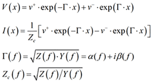
Eq. 2
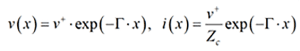
Where Zc is complex frequency-dependent characteristic impedance and gamma is complex propagation constant (alpha is the attenuation constant [Np/m] and beta is the phase constant [rad/m] defined as 2*PI/Lambda, and lambda is the wavelength in the transmission line – phase changes by 2*PI over that length – see more in the Appendix).
Those are the modal parameters in general; the equations above are for a two-conductor line with one mode only. If we write the solution for the wave propagating only in one direction along the x-axis, for instance (as would be ideal for signal transmission):
Eq. 3
We can see the characteristic impedance is just a ratio of the voltage and current of the wave propagating in one direction of transmission line v(x)/i(x)=Zc. It is impedance by dimension (ohm). It is pure resistance if the line is lossless. “Characteristic” is used here because it does not depend on the position or length of the transmission line segment (independent of x), it “characterizes” it. It depends only on the type of transmission line and geometry of the cross-section. Note that for planar transmission lines, used for PCB and packaging interconnects, the definition of impedance is not unique and can be done three ways: through voltage and current, current and power, and voltage and power, but all are close to the conventional “static” voltage-current definition if the cross-section remains much smaller than the wavelength, which is usually a good assumption for PCB and packaging interconnects.
To investigate the reflections, the next step is to define properties of a transmission line segment. The telegrapher’s equations introduced in the previous section are incomplete without the “boundary conditions” or terminations. The most effective way to describe a segment is to use waves and scattering parameters or S-parameters. Here is a transmission line segment with length l connected to voltage sources with all variables, to define S-parameters:
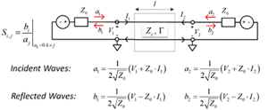
Eq. 4
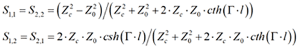
Where a1, a2 are the “incident waves,” and b1, b2 are the “reflected waves” with dimension sqrt(Wt). V1,V2 and I1, I2 are voltages and currents at the segment ports (pairs of terminals). Zo is the termination or normalization impedance (the same thing, in this context). Waves in this definition are not actual waves in the transmission line, but rather variables formally defined through voltage and current. Using equations for voltage and current in transmission line segment (superposition of two waves defined earlier) and Kirchhoff’s laws at the external terminals or by following more formal procedure from Pupalaikis4, we can define S-parameters or S-matrix that relates the incident and reflected waves for such segment as follows:
Eq. 5
The reflection (S11 and S22) and transmission (S12 and S21) can be expressed separately as follows:
Eq. 6
Note the transmission parameters include the effects of the absorption and reflections: these expressions have no approximations. This is a universal definition of reflection and transmission; it can be used for simple experiments with transmission line properties or as rigorous modelling of a segment. It depends on the definition of characteristic impedance and propagation constant used. The rest is pure trigonometry! You can start with a frequency-independent capacitance and inductance per unit length or use more complicated expressions for the characteristic impedance and propagation constant such as used in Simberian App. Note #2012¬¬_02.5 For simple experiments, the propagation constant can be defined analytically with formulas or simply with phase delay or propagation velocity for ideal lines (see Appendix). This is very simple and an important tool for all kinds of experiments in the frequency domain with real transmission lines. It includes all reflections in time domain (if model bandwidth is properly defined per Shlepnev1)! Nevertheless, use of frequency domain response for time-domain analysis is not as easy.4 Simbeor software is used here for all frequency and time domain analyses as it makes our investigation much easier.
Now, what useful information can be derived from such a simple trigonometric model? Let’s begin from a very simple case of the termination or normalization impedance equal to the characteristic impedance Zo=Zc – the reflection parameter is zero in this case as we can see from the formula! The S-matrix in this case is particularly simple and defined as follows (generalized modal S-parameters):
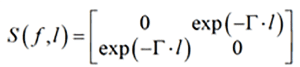
Eq. 7
Only the transmission parameters and no reflections! This should be the Holy Grail of the interconnect design: the signal is traveling strictly in one direction. The signal, however, may still not get through because the transmission parameter depends on the absorption and dispersion in gamma (discussed earlier in Shlepnev2).
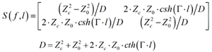
Considering the zero-reflection condition, why we do not do it like that all the time? First, the characteristic impedance is complex for lossy lines – it has real and imaginary parts. The zero-reflection termination is not just a resistor, it should be frequency-dependent. But this is not the showstopper. The real part of the characteristic impedance does not change the important frequencies much at all and the imaginary part is much smaller than the real part, as we can see from the plot in FIGURE 1:
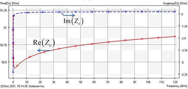
Figure 1. A typical PCB case showing real and simulated characteristic impedance.
At least theoretically, we should be able to get very close to the nonreflective case. Practically, there are more factors that do not allow it – the manufacturing variations and discontinuities such as pads and via holes are the most important ones.
Now, armed with the theory, let’s investigate a simple 5cm stripline segment with characteristic impedance about 50.4Ω at 1GHz (changing with frequency as shown above) on FR-408 simulated as Wideband Debye with Dk=3.8, LT=0.0117 @1GHz, copper with RR=1.2, Causal Hammerstad Roughness Model: SR=0.4, RF=2. The problem is as realistic as can be and the only simplification is the absence of discontinuities.
FIGURE 2 shows the transmission line segment response in frequency and time domains (computed with Simbeor software).
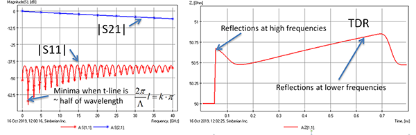
Figure 2. The transmission parameter magnitude is smooth and is defined mostly by the absorption by dielectric and conductors.
Both ends of the transmission line segment are terminated by 50Ω (exactly). Magnitudes of the reflection |S11| and transmission |S21| parameters are shown on the left plot and corresponding TDR on the right plot (reflection from 20ps step response in Ohm). S-parameters are shown in dB (20log(|S11|) and 20log(|S21|)). First, we can observe that the reflection is not zero, but very low: below -37.5dB (only about 13mV is reflected with 1V excitation, as good as is usually not possible).
Consequently, the transmission parameter magnitude is smooth and is defined mostly by the absorption by dielectric and conductors. Notice that the reflection parameter has some minima and maxima. The first maximum is at a frequency where the segment length is about equal to a quarter of the wavelength in the transmission line, defined by Gamma (see Appendix) and repeating every half of the wavelength. The first minimum is at about half of the wavelength and is repeated every half of the wavelength (explained below). The value of the reflection at one frequency point may be misleading. Considering the TDR, we can see that it shows some variations consistent with the variations of characteristic impedance – see more on that at Simberian App. Note #2009_04.6
What if the characteristic impedance of the transmission line is significantly different from the termination impedance? Let’s look at about 25Ω stripline in the same stackup as above (FIGURE 3).
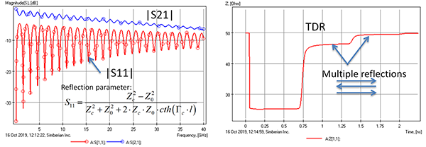
Figure 3. In this example, reflection went up considerably, meaning more signal energy is reflected. As result, the transmission (insertion loss) went down at some frequencies.
Magnitudes of the transmission (insertion loss) and reflection in dB are shown on the left plot and TDR on the right. The reflection went up considerably, meaning more signal energy is reflected. As a result, the transmission or insertion losses went down at some frequencies: less signal energy is transmitted. The insertion loss is now wavy and repeats the reflection pattern – the maxima in the reflection are the minima in the insertion losses. The signal energy here is either reflected or absorbed. The left plot also has the expression for the reflection parameter. The hyperbolic tangent in the denominator explains the minima and maxima: it is trigonometry! (Although with complex numbers.) S-parameters are used directly to compute the TDR, which in this case shows multiple reflections from the ends of the segment.
Another case with considerably larger characteristic impedance of about 75Ω (cannot be exact) and same segment length and 50Ω terminations is shown in FIGURE 4.
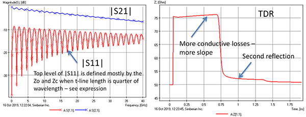
Figure 4. This example has more conductive losses, and the narrow transmission line shows more resistance.
On an S-parameter plot, it looks very similar to the previous case. It has more conductive losses, however, and the TDR goes up instead of down, and shows more resistance (slope up) in the narrow transmission line as expected. In both “reflective” cases, only one or two reflections are significant – it disappears quickly due to the absorption losses (losses are our friend in such reflective cases).
If you are wondering why a characteristic impedance equal to 50Ω is usually selected for single-ended and 100Ω is selected for differential PCB or packaging interconnects, you are not alone. It can only be explained by the historic reasons and convention for the component terminators. In fact, there are no reasons to stick with this number. As the story goes, 50Ω was the tradeoff impedance of an air-filled coaxial transmission line between the maximal transmitted power and minimal losses.7 Indeed, a coaxial line always has a minimum in losses versus impedance. Though it is dependent on the dielectric fill, it happens to be close to 50Ω for coaxial lines filled with PFTE-type dielectric with Dk close to 2 (this can be easily verified7). As we know, striplines are descendants of the coaxial transmission lines, but the stripline losses do not have a minimum on the loss versus impedance function. FIGURE 5 shows the attenuation in dB/m for a stripline modeled with Dk=3.5, LT = 0.002 @1.0e9, Huray-Braken roughness model: SR = 0.1μm, RF = 9 as a function of dielectric thickness and characteristic impedance at 10GHz (computed with Simbeor SDK for Matlab).
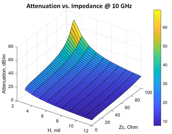
Figure 5. Attenuation (in dB/m) for a stripline model.
The attenuation is simply smaller for the smaller characteristic impedance (Zc axis) as well as for the thicker dielectrics (H axis). As was shown in Shlepnev2, the conductor losses dominate in striplines with very-low-loss dielectrics. It means the cross-sections with more metal and lower impedance have smaller losses in general. The single mode propagation condition and layout density, however, may put additional bounds on the increase in cross-section size and on the lowest impedance as well. So, is lower impedance always better? Not really, if our goal is to minimize power absorbed by the interconnects and terminators. For instance, if we need a 0.1V signal at the receiver and compute power required at the transmitter side (Pin=20log(Vout)-10log(|Zc|)+Att_dB*Length, dBW), we will see some minima (same example as above at 10GHz, computed with Simbeor SDK for Matlab) (FIGURE 6).
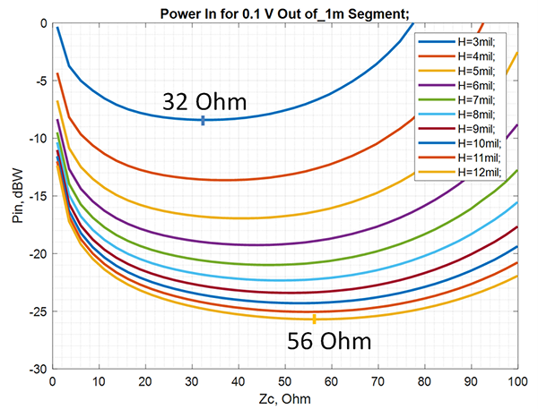
Figure 6. The minimal power depends on the geometry and length, with smaller impedance considered for thinner dielectric layers.
The minimal power depends on the geometry (dielectric thickness H above and below trace and trace width adjusted to have impedance value on the horizontal axis) and length (the graphs shown in Figure 6 are for a 1m segment). Smaller impedance should be considered for thinner dielectric layers. Strip widths in this example are set to have the impedance shown on the horizontal axis (Simbeor SDK used for computations). Terminations in this case were set equal to the magnitude of the characteristic impedance at 10GHz (no reflections). As we can see, the lower characteristic impedance is not always better and may be optimized for a particular system.
Finally, constant impedance from component to component should be the design goal, but it is usually violated in practical cases. The single-ended or differential traces are the open waveguiding structures composed of traces and reference conductors, although almost all layout tools are not aware of that. As such, prior to any type of interconnect analysis, impedance continuity should be verified with a validated field solver. FIGURE 7 shows an example of such impedance verification for CMP-28 validation platform from Wild River Technology (wildrivertech.com) in Simbeor 2022.02.
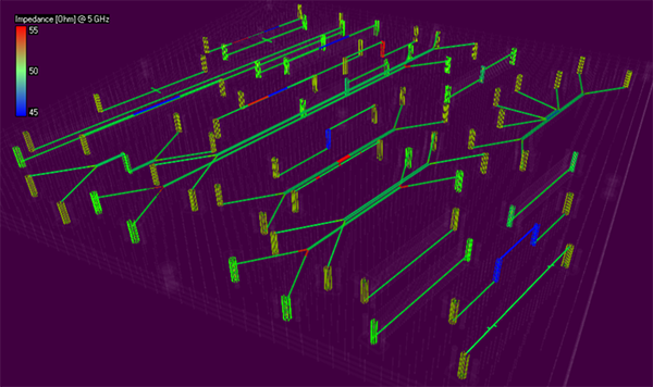
Figure 7. Impedance continuity as verified with a validated field solver.
Green is used for objects with an impedance close to the target impedance (50Ω single-ended or 100Ω differential). Objects with impedance below the target are blue and with higher impedances are red. This is a well-designed board with a small number of intentional impedance violations in some structures. Also, it comes from Wild River Technology, with measurements up to 50GHz for validation purposes.
Another example of how the reference conductors can change the impedance of traces on a design with traces going through BGA breakouts is provided in FIGURE 8.
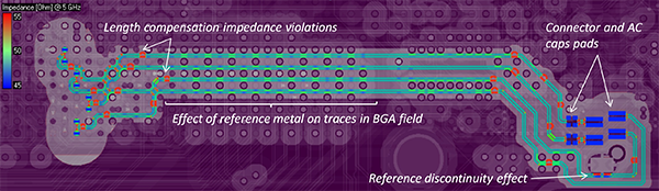
Figure 8. Another example of how reference conductors can change the impedance of traces on a design with traces going through BGA breakouts.
Here, we evaluated the effect of cut-outs and reference pads on impedance; those cannot be avoided. We can see the impedance of the connector and AC coupling pads is below the target and the impedance of the length compensation sections is above the target (a layout mistake). The discontinuities in the reference conductors also create impedance violations (another layout mistake). Most of those violations may not kill the signal and are important at relatively high data rates, however.
References
1. Y. Shlepnev, “How Interconnects Work: Bandwidth for Modeling and Measurements,” Simberian App. Note #2021_09, Nov. 8, 2021.
2. Y. Shlepnev, “How Interconnects Work: Absorption, Dissipation and Dispersion,” Simberian App. Note #2021_10, Nov. 26, 2021
3. Y. Shlepnev and V. Heyfitch, “Design Insights from Electromagnetic Analysis & Measurements of PCB & Packaging Interconnects Operating at 6- to 112-Gbps & Beyond,” DesignCon, January 2020.
4. P. J. Pupalaikis, S-parameters for Signal Integrity, Cambridge University Press, 2020.
5. “Can Conductor Roughness Effect be Accounted for in Dielectric Model?” Simberian App. Note #2012¬¬_02.
6. “Micro-strip Line Characteristic Impedance and TDR,” Simberian App. Note #2009_04.
7. Microwaves 101, “Why Fifty Ohms?” microwaves101.com/encyclopedias/why-fifty-ohms.
Appendix
Other useful transmission line modal parameters derived from the complex propagation constant (Gamma) and useful for understanding of transmission line behavior (omega is the radial frequency [rad/s]):
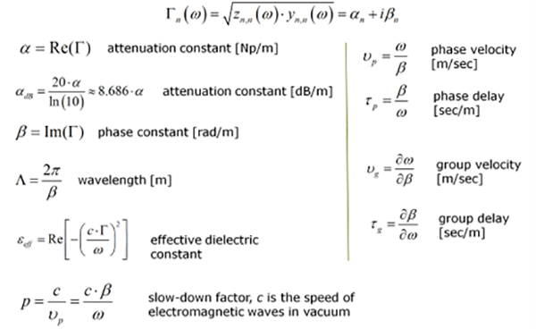
Appendix Equation
Yuriy Shlepnev is president and founder of Simberian (simberian.com), where he develops Simbeor electromagnetic signal integrity software. He has a master’s in radio engineering from Novosibirsk State Technical University and a Ph.D. in computational electromagnetics from Siberian State University of Telecommunications and Informatics. He was the principal developer of electromagnetic simulator for Eagleware and a leading developer of electromagnetic software for the simulation of signal and power distribution networks at Mentor Graphics. His research has been published in multiple papers and conference proceedings; This email address is being protected from spambots. You need JavaScript enabled to view it..


