Not leaving enough clearance is a design oversight that can have costly consequences.
As PCB designers, fabricators and assemblers, we wear a lot of hats at Rush PCB. We're always working to design and build PCBAs that are the best they can be. But sometimes we are consigned product to assemble that wasn't designed by our team, and every so often we get boards that tempt us to say, "The designer clearly wasn't thinking about how we are going to build this!"
Design for manufacturing (DfM) principles are critical, and can make the difference between an assembly that is easy to build and one that is nearly impossible. As SMT PCBs become more compact, and components are large or odd-form, designers need to account for the special needs and limitations of the automated assembly equipment in the workstations, because few – if any – assemblies can be cost-effectively assembled by hand. It's always important for electronics designers to talk to the manufacturing engineers at the assembler where the parts will be consigned. Working together saves a million headaches.
In one instance, we were consigned to build a PCB assembly that, upon examination, had zero edge clearance. How is that possible? The assembly had five edge mount connectors (PMolex 1-5) that extended out from the board approximately 1.5mm on each of the four sides of the board. But all the equipment we use to assemble products must be capable of holding the board by at least two of its edges and require a clearance of approximately 5-10mm. As a result, these PCB assemblies had effectively zero edge clearance, as shown in FIGURE 1, where the interference caused by the connectors is obvious.
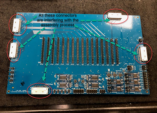
Figure 1. Processing the PCBA is impossible with large connectors in the way. Processing equipment requires appropriate edge clearances.
As a result of this design oversight, the assembly process would have been very difficult – if not impossible – because we couldn't hold the PCBA properly and some of the connectors contacted or "bumped" the reflow conveyor. That is unacceptable because it could result in component misalignment or open solder joints, requiring costly rework and delaying shipping deadlines. Not leaving enough clearance is a design oversight that can have costly consequences.
Mission: Impossible? Not really, because this case had both a great solution and a not-so-great one. In the first and best solution, 10mm wide breakaways could be added all around the edges of the board and connected with 2.5-3mm long "mouse bites." This solution, shown in FIGURE 2, would speed the assembly the process, protect the connectors, and prevent the need for rework due to misalignments or open solder joints.
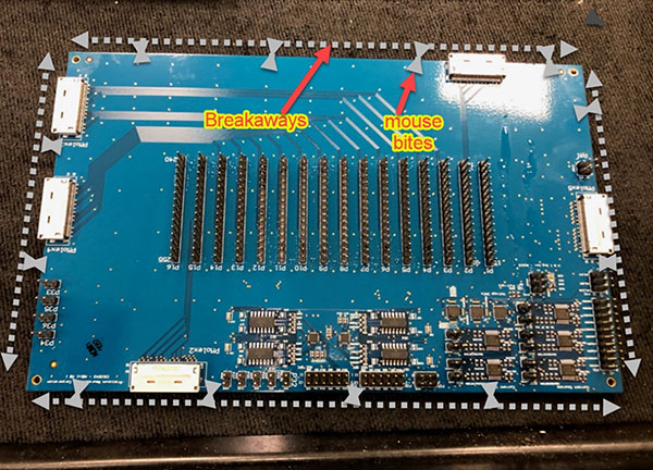
Figure 2. Breakaways and "mouse bites" to hold them in place eliminate the need for fixturing and potential rework while providing needed edge clearance.
The less-desirable solution would be to ask the customer to pay for fixtures to accommodate the PCBAs for passage through the pick-and-place, reflow and AOI systems. Clearly, the first solution described would be better since it is cheaper than fixturing.
Akber Roy is chief executive officer of Rush PCB Inc., a printed circuit design, fabrication and assembly company (rushpcb.com); This email address is being protected from spambots. You need JavaScript enabled to view it..


