Embedded passives are being deployed for commercial market applications.
Recent advancements in mobile technologies have exponentially increased demand for radio spectrum bandwidth. The rush of equipment for more RF applications is being deployed across the world, with 5G and millimeter wave (mmWave) communications expanding into the commercial space to take advantage of the wider bandwidth, higher data rates and low latency that these frequency bands offer. Cellular 5G and 6G, low Earth orbit (LEO), mid Earth orbit (MEO), geosynchronous communications networks, interconnected devices (internet of things), autonomous driving vehicles, defense and environmental monitoring are all driving these needs. The antenna and sensors necessary to manage the signals for these applications are similarly changing, becoming more sophisticated.
To ensure high-data-rate wireless connectivity, the broadband high-gain antennas necessary to manage high-frequency but lower-power signals are increasingly moving from dish and horn to flat-panel active electronically steered antennas (AESA) for beam forming and massive MIMO designs. In response, the RF industry has developed new integrated circuits, materials, processes and equipment to build devices to manage these mission-critical sensor applications.
Much of the development and understanding of how to engineer and build reliable and accurate transmit-and-receive sensors for today’s environment were derived from phased array antennas and Ka/Ku-band radar engineering typically used in defense applications. The AESA products being developed can shape azimuth, elevation and antenna pattern as desired to generate beams that target specific communications devices.
Embedded resistor copper foils have a long history of applications in military/defense antenna systems and remain well positioned to support the design and manufacture of the flat-panel, PCB-based AESA antennas necessary to handle this expanded antenna paradigm.
As AESA technologies used in the defense and space sectors are deployed for commercial applications, designers who may not have broad experience in implementing systems with this technology are faced with a must-have list of printed wiring board concerns, including tighter routing, higher layer counts, maximum surface area for components, the lowest possible insertion loss and system-acceptable attenuation characteristics.
As 5G and mmWave communication are leveraged by the commercial marketplace, system architects and designers envision thousands of flat-panel AESAs discreetly mounted across the landscape. As frequency rises, so do the limits of the RF waves to travel through space, objects and variable environmental conditions. As a result, more antennas, repeaters and base stations are necessary to mitigate signal attenuation, coupled with lower power and shorter propagation distances at these short wavelength frequencies.
One antenna technology design option is using thin-film copper foil technology incorporating embedded passive materials. Embedded passives can be slimmed-down SMT components built and mounted into the inner copper and dielectric layers of the PWB laminate substrates. Embedding components allows designers to create smaller PCB/package sizes with better signal integrity and gain increased board surface space for active component mounting because of a more efficient wiring design. While components and mounting technologies are evolving to meet the challenges of discrete devices within PWBs, embedding thin-film-based resistors etched and formed within the copper foil traces leverages decades of effectiveness and robustness, no additional component buying and stocking, no extra handling and placement of components, elimination of wire bonding or solder processes within the depths of the PCB during the processes of multilayer build, and no cavity or added space requirements and potential component waste should the subsequent multilayer laminations go awry. Embedded thin-film resistors further enhance reliability of PWBs in part due to the aggressive sealing measures employed during the PCB’s lamination processes.
Thin-film embedded resistors address many of the needs of SMT passive resistors, while providing additional value that can be factored into the overall completed PCB cost model. Given the PCB layers must have copper routing lines and spaces to move signals to and from active components, the resistor materials residing beneath those traces, while not free, are already in place to be used to lower PCB costs.
Due to the thin nature of embedded resistors (200-10000Å, 0.02-1.0µm), the resistors can be buried in innerlayers of printed circuit boards without increasing the overall thickness of the board. To do so, they employ internal cavities or occupy surface space for discrete SMT resistors (FIGURE 1). These resistor networks become part of the etched and printed circuitry on the standard PCB layers, thereby eliminating the need for passive SMT resistors and the many solder connections, bonding issues and routing vias servicing those components. Resistor foils are alternatives to traditional termination and pullup/down SMT resistors and widely utilized for balancing resistors in Wilkinson power dividers. By removing discrete SMTs from PCBs, interconnecting traces and vias claim less room, so engineers can add other functions and reduce the PCB size for smaller, higher frequency applications and systems.

Figure 1. Embedded passives can be placed in cavities and become part of the circuitry.
Millimeter and higher frequencies mean smaller and more tightly routed microstrip and stripline circuit designs and reliance on stable Dk and Df high-frequency PCB dielectrics, smoother, thinner copper foils, and other advanced technologies to limit signal degradation. Thin-film embedded resistive material technology offers a solution for many high-speed, low-loss, high-frequency applications where absolute performance and reliability are essential.
Designing with Embedded Resistors
Among the myriad design decisions that must be made – function, size, interconnection with other boards, laminate materials, thermal issues and components used – designers need to decide if they intend to use buried resistors at the frontend of the process.
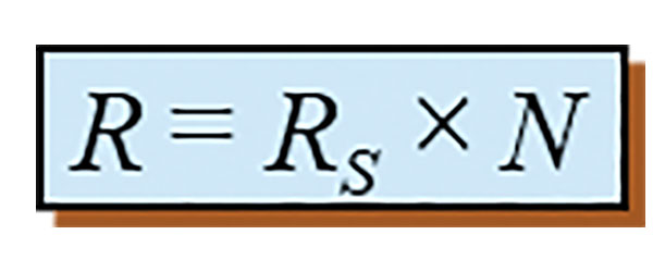
The basic design concept for embedded resistors can be seen in the following equation:

EQ. 1.
where Rs is the sheet resistance of the resistor material designated as ohms per square (OPS).
The resistance value can be determined by material resistance and geometry of the resistor according to the formula above.
EQ. 2.
where N is the ratio of length to width or number of squares (N = L/W).
- For a given sheet resistivity:
- Resistance of a square area equals the bulk sheet resistivity of the material.
- One square of 25Ω/□ material will equal 25Ω regardless of the size of the square.
- To create different resistor values with a given sheet resistivity, adjust the length-to-width ratio or number of squares.
- For example, to create a 50Ω resistor using Rs of 25Ω/□ material, adjust the length to twice the width:

Figure 2. Resistance value is established in part by resistor geometry.
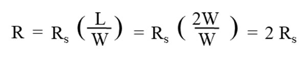
EQ. 3.
Resistors can be patterned as bar type using multiple squares and further arranged in a serpentine type of multiple squares. They can also be designed circular or form an arc.

Figure 3. Resistor patterns include a bar type with one (3a) or more squares (3b), as well as a serpentine pattern (3c).
Embedded resistor suppliers provide design tools in which the engineer can select resistance, power handling and tolerance to suggest the appropriate resistor dimensions.
Power dissipation, temperature rise and laminate substrate used all have an effect of the working life and long-term stability of the resistor. In general, the larger the resistor area the better, especially in designs where power and reliability are critical.
Manufacturing embedded resistors with resistive copper foil involves two print/image and develop steps and two or three etch steps, depending on the resistor alloys being used. Standard resistor alloys are nickel chromium (NiCr), nickel phosphor (NiP), silicon (Si), aluminum (NCAS) and chromium silicon monoxide (CrSiO). Considerations include the equipment setup for the photoresist application and subsequent exposure and development, as well as process control for selective copper removal to define resistor length. These processes can impact individual resistor tolerances. The inclusion of the resistive foil layer between the substrate and copper layer and the print and etch process steps result in resistors having customized ohmic values embedded inside PCBs after the PCB lamination process.
The OPS sheet resistance for sputtered and plated copper foils in roll form are controlled to a plus or minus 5% coefficient of variance value. The manufacturing process is calibrated using precise measurement and SPC guidelines. The roll-to-roll sputter and/or plated manufacturing produce a thin, continuous, conformal resistor alloy coating that mirrors the profile of the matte side of the copper foil. Trace width, conductor spacing and etch rates are predictable to maintain consistency with most modeling and design software. This eliminates the need for excessive iterative engineering to move from design to realized products.
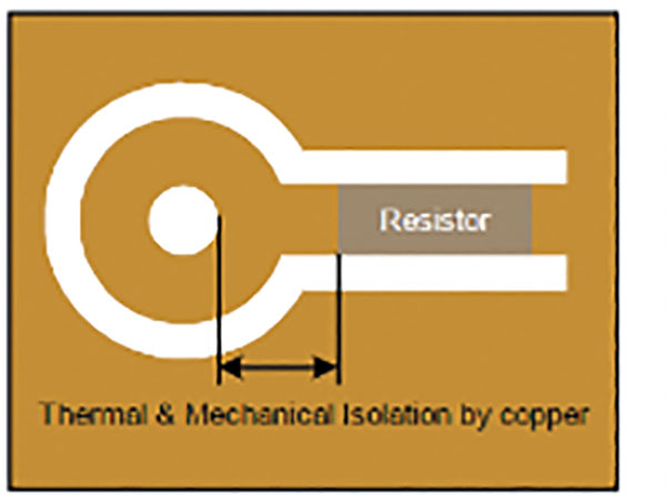
Figure 4. The resistor in the ground plane requires an isolation area between the ground plane and the resistor. (Source: Ticer Technologies)
Embedded resistor foil products are available in roll form and customer-specified sheet sizes. Foils are produced at a 51" or 40" width cross-web standard, and production rolls are hundreds of LF in the down-web direction. This allows users to work with various combinations of dielectric laminate cores or PCB innerlayer layup processes. This flexibility allows users to scale to their preferred and most economical unit size. Foils come in a range of standard resistor options from 10 to 1000Ω per square bulk sheet resistance.

Figure 5. Processes for defining resistor elements. (Source: Ticer Technologies and Coretec)
As signal speed increases, so does the skin effect causing the electrical energy to move nearer to the surface of the copper traces in a PCB. At these higher speeds, roughness profiles and etching quality of embedded resistor foils are critical to achieve the best possible insertion loss characteristics. Furthermore, line, space and etched microwave structures like Wilkinson power dividers must become smaller to manage the wavelengths.
The final resistance tolerance is a function of delivered tolerance, the relative movement up and down in value during dielectric lamination (annealing effect) and the precision of the copper and resistive material etch processes of the PCB fabricator. Precise etching process controls repeatedly produce resistors with good tolerance.
Thermal Dissipation Factors
All aspects of the system’s thermal dissipation must be considered in the PCB design. Factors that affect thermal dissipation in the system are circuit configuration; circuit thickness and material type; thermal conductivity of the dielectric; proximity of power or ground planes to resistors; ambient temperature; additional system cooling or heat sinking; and resistor size (total resistor area).
All electronic systems need to consider cost. This is particularly important as technologies developed for defense applications are adopted for commercial applications. Understanding the total system cost drives designers to consider options, including embedded passives. Designers need to consider tradeoffs, such as using thin-film embedded resistor foils to place most or all of the resistor networks on a layer or two inside the board in place of SMT components. They need to decide if reserving more surface real estate, simplified packaging and improved signal integrity by using embedded resistor foils would lower the overall cost of the system vs. standard SMT devices.
Thomas Sleasman is manager, sales and marketing, at Ticer Technologies (ticertechnologies.com); This email address is being protected from spambots. You need JavaScript enabled to view it..


