High-speed circuits are used more or less everywhere in electronic applications today.
As a result, the importance and the mechanisms of impedance (here in the meaning of PCB trace impedance – typically referred to as “characteristic impedance”) for signal integrity have been widely discussed and seem to be generally well understood by PCB designers.
Simply put, PCB trace impedance is a measure of the resistance that a circuit opposes to a current once a voltage is applied. So far so good, but the concept of impedance is also used in PCB design to describe the behavior of power-distribution systems/power distribution networks (PDS/PDN). And this PDN impedance is becoming more and more of a headache for PCB designers as IC vendors are defining increasingly tight so-called ‘target impedance limits’ that a design must meet (a few milliohms over a broad frequency range).
You are not sure what the term PDN impedance actually means for you and what you have to pay attention to when designing a PDN? Let’s take a look at what PDN impedance and target impedance are and let me take a stab at explaining their importance for the design of modern high-speed digital boards.
Impedance and its Relation to Capacitance and Inductance
The theory of electronics plays an elementary role in analyzing impedance issues, just to mention here Ohm’s law, Kirchhoff’s laws, and for inductance Faraday’s laws. But even without diving in too deeply, PCB designers know that for board traces the characteristic impedance “Z0” is directly related (lossless case here for simplicity) to the trace inductance (L) and the trace capacitance (C), or in formula definition:

Hence, the trace capacitance depends directly on the trace construction within the board: trace width, copper height, and the trace’s distance to a reference layer acting as a return path. The dielectric constant “ε” of the surrounding insulation material also has its impact. Knowing this, it can be rather simple to predict the effects of certain physical construction changes on the trace impedance value by analytical formulas.
However, for closely coupled traces and trace geometries with etching and copper roughness impact, such a prediction can become quite complicated. PCB engineers should always keep in mind, that the relationship between capacitance and impedance is somehow inverse, which means that if “C” increases, “Z0” decreases and vice versa. But how does this apply to power distribution systems?
Power distribution systems typically comprise a combination of larger (and/or smaller) copper areas together with power traces, PDN-vias, and many small connection stubs to carry energy from the power sources (bucket converters, VRMs, or PMICs) to the active circuits (ICs) – with some discrete components (capacitors, resistors, inductors) in between. So how and where does impedance come into play?
Introducing PDN Target Impedance
As clock and data frequencies increase and high-speed boards become densely populated with increasingly power-demanding integrated circuits (pin-counts rising to over a thousand pins), ensuring a noise-free power distribution from the source to the sinks becomes a major challenge for any PCB designer.
Typically, many IC buffers on a board simultaneously change their state. These fast-switching devices cause ripple voltages that propagate through the entire power distribution network and create noise peaks. These vary in frequency and location on the board. As we learned in school, energy will never just disappear. Therefore, the noise (=energy) can easily disturb any surrounding high-speed devices and circuits. Ripple voltages can also be strong EMI sources, creating high-impact parasitic EMI antennas through conductive coupling.
In switching mode, where there are voltages and current flows, the ratio between these two values forms the impedance of a PDN like the simplified one pictured below (FIGURE 1). For the sake of simplification, only the plate capacitance of the planes is shown, just as not all different inductances are included in the picture either.

Figure 1. Simplified schematic structure of a PDNX.
One approach to ensuring the proper operation of high-speed systems while maintaining the required performance is to control the power delivery network impedance over a certain frequency range (FDTIM=frequency domain target impedance method). This can be achieved by carefully designing the structure of the power distribution network and taking into account the total PDN capacitance and all various inductances. The overall capacitance number goes beyond the plate capacitance of the power-ground overlap areas and includes bulk capacitance of the large capacitors, all the decoupling capacitance and at the end, the embedded capacitance within the IC packages and the IC die itself.
The most straightforward approach to explain the impedance of a PDN is:

If we take a closer look at the frequency behavior (see FIGURE 2), it becomes clear that any PCB power delivery network will show some degree of capacitive behavior at lower frequencies while this capacitance decreases due to the resistance of the power-bus in series with all the load components and its return path and then the inductive behavior typically dominates. Figure 2 shows all impedances vs. frequency for a NXP iMX55 CPU for a DDR3 power rail of an automotive ECU for all the CPU power pins.
The impedance is affected by the physical separation within the power rail in the board stackup. As frequencies increase, the mutual inductance between the different circuits on the board will cause the impedance of the power distribution network to increase. Due to various effects, the impedance of such a structure shows many peaks (resonances and anti-resonances). At higher frequencies, the impedance often negatively influences the input behavior of the ICs, which is highly undesirable especially in the frequency range in which the ICs are supposed to operate.

Figure 2. Impedance vs. frequency (Z(f)) of a PDN of an NXP iMx5 CPUX.
Target Impedance Values in PDN Design
The knowledge and control of the target impedance have become a standard approach for proper PDN design, especially when designers must meet the given IC vendor or application specs. A target impedance, by definition, sets a limit on the highest impedance the power rail on the die may be exposed to in its connection to the PDN.
Different formula approaches, all based on Ohm’s law, state that the ratio of voltage to current results in the resistance (=impedance). For a PDN, the voltage in these formulas is the supply voltage in relation to the maximum ripple (∆V) on the power supply which ICs are allowed to accept (IC vendors have this information). In its simplest form, the target impedance can be described as:
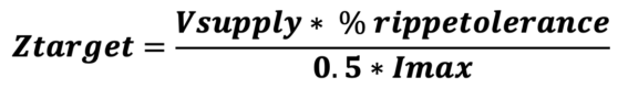
Hence, the target impedance can be understood as a limit of the current/voltage ratio to ensure, that the ∆V from Equation 2 does not exceed the desired ripple voltage limits. If the PDN impedance stays below the calculated value, even the worst-case transient current from the IC die will generate just a rather small rail voltage noise which is still acceptable for operation.

Figure 3. Example of IC vendor target impedance limits (Source: Qualcomm).
The impedance waveform of a power delivery network should ideally be without larger peaks within the frequency band in which the ICs operate. This is the fundamental guiding principle in the target-impedance-based design approach of PDNs. Another matter of concern is the relevant bandwidth. For digital signals, the bandwidth comprises all frequencies between the clock and the knee point on a frequency curve (which can in a rule-of-thumb approach be defined as 0.35 divided by the fastest signal transient rise/fall time).
If all the harmonics of digital signal resonate at the same frequency, the transfer function for the return signal in a ground plane will be rather flat which is what we are looking for. For a really complex PDN, every occurring impedance peak is created by a parallel RLC circuit. The characterizing terms for such impedance peaks are:
- Parallel resonant frequency
- Characteristic impedance (and the q-factor, not discussed here)
- Peak impedance.
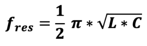
The parallel resonant frequency defines the frequency, at which the inductive reactance equals the capacitive reactance. This frequency point can be calculated from:
When a transient voltage occurs at the resonant frequency of the peak, the amplitude of the resulting voltage swing may exceed the nominal voltage given by the target impedance equation. To further complicate the matter, often there are further impedance peaks (→ multiple resonances and anti-resonances) over a wider frequency range to deal with.
Not every peak that exceeds the target value would mean, that the system is not working. However, the peaks could lead to non-deterministic IC power failures during system operation. This opens a Pandora's box for debugging such hardware failures. But even if the peak stays below the impedance limits, the circuit may not be perfectly safe, so countermeasures may be required to lower the impedance or shift occurring peaks in frequency.
First Aid Kit to Lower PDN Impedance
The idea behind FDTIM is to ensure that the PDN design meets the target impedance and the values for the relevant frequency range stay below the given limits. Yet this is easier said than done. A PCB usually contains dozens of active components, often several hundred capacitors and inductors with all their parasitic characteristics (e.g., ESL and ESR of the capacitors). There are also other parasitic inductors on the different PDN elements (e.g., pads/land patterns, vias, and traces) that can heavily affect PDN impedance values.
To lower the impedance of the PDN, engineers can tweak two general things: reducing the inductance and/or increasing the capacitance of the PDN. The placement and value of decoupling capacitors play an important role in such an optimization, as this will affect both, the capacitance and the inductance of the PDN. Placing the capacitors on the same layer as the IC supply pins, for example, minimizes the inductance. Unfortunately, this is often not possible for space or manufacturing reasons. Nevertheless, if resonance peaks are revealed in a PI analysis, the copper shapes of the PDN most likely have to be modified to eliminate these peaks efficiently.
Unfortunately, given the complexity of today’s PDNs and all the parasitic effects, analyzing a circuit layout for PDN impedance can hardly be done with a good old pen and a sheet of paper. Furthermore, PCB CAD tools cannot handle target impedance issues simply by defining a design rule or adding an attribute to a power supply network, even if this is desirable for the PCB designer.
Instead, advanced engineering tools like numerical PI solvers are needed. Such simulators have been available on the market for many years. An easy exploration and verification of power distribution systems are possible as an integral part of the PCB design process. In lowering the power distribution network impedance across the required range of frequencies, potential EMI issues can be eliminated too.

Figure 4. Impedance mask definition to check IC vendor rule compliance using the Zuken PI Simulator.
If such an analysis reveals resonance peaks in a PDN exceeding the target impedance, corrections can be engineered in a virtual sandbox through the parametric study capabilities of some ECAD tools. Such corrections, for instance, include adding virtual decaps, changing values and ESL of the capacitors, or even turning them OFF without the need for physical design changes in the tool.
Conclusion
This concurrent PI analysis approach helps PCB designers avoid overengineering a PDN. An overly cautious approach typically results in adding redundant capacitors and extra validation hours, which translate into unnecessary costs.
As a final reminder, digital engineers should always keep in mind that the situation is often even worse than initially thought (→ Murphy’s law). Power integrity issues such as impedance resonance peaks negatively influence the signal integrity behavior of boards. And in their nature as a (rather very large from the physical size of the structure) LC-resonator, a noisy PDN can easily become a strong parasitic EMI antenna. This underlines the importance to keep the PDN impedance number under control.
References
1. Eric Bogatin, Signal and Power Integrity Simplified, 2009.
Ralf Bruening is a product manager involved in the development and deployment of Zuken’s analysis and high-speed solutions for the past 20 years. Ralf works to improve customer design processes and solve complex technical challenges associated with high-speed signal transmission, power integrity problems, and EMI emissions. In his free time, Ralf likes to golf, cook for his family and listen to rock music. He will speak at PCB East in Marlboro, MA, in April 2022.
Ed.: The original publication displayed an incorrect formula for the impedance of a PDN. We regret any confusion.


