Once energy leaves a controlled path, the chances are it will cause interference and radiate from board edges.
The energy that flows on a logic circuit board leaves as heat and/or electromagnetic radiation. As clock rates have risen, radiation has become more of an issue. The logic voltage levels we view are at the end points of transmission lines. To move logic signals we need to understand how nature moves energy. There are no energy meters, so we must rely on theory to understand how to limit radiation. This is the same theory that governs all electrical behavior. The control of radiation is not complicated but it is different than circuit theory.
Consider a transmission line consisting of a conducting trace over a conducting ground plane. The trace is separated by a layer of dielectric. When a voltage is switched across the line, an electric field begins to appear in the space between the two conductors. A very small part of this electric field is located in the conductors. This small field causes current to start flowing in the conductors. This current is associated with a magnetic field that occupies the same space as the electric field. The voltage and current rise in value is what is called a leading edge. This leading edge moves down the transmission path. The time it takes for the voltage to reach 90% of final value is called the rise time. The motion of the leading edge is called a wave. The ratio of voltage to current flow is called the characteristic impedance of the transmission line. It is typically 50Ω. The wave velocity in a typical dielectric is half the speed of light.
Energy Flow on Transmission Lines
The flow of energy is in the electric and magnetic field behind the leading edge of the wave. These fields are in the space between the two conductors. We can measure the electric field by noting the voltage across the line. In theory, we could measure the magnetic field by using a small compass. Note that behind the wave front, the two fields are static and coupled together. If the line is short enough or if the rise time is long enough, the wave will reach the open end of a transmission line and not reflect. The capacitance of the line will store energy defined by the initial voltage: 1/2 CV2. When the switch returns the initial voltage to zero, the energy stored in the capacitance is dissipated mainly in the resistance of the logic switch.
If a transmission line is shunt-terminated in its characteristic impedance, there is no reflection, but there is dissipation in the resistor as long as the logic voltage is present. If the transmission line is series-terminated at the logic source, the logic voltage is halved. At the open end of the line the half voltage doubles, and there is a reflection. This reflected wave is terminated at the source and all wave action stops. The preferred approach is to limit the path length or increase the rise time to avoid a reflection.
The energy that flows on a transmission line flows in the space between conductors. In a good logic layout design, every logic signal uses a dedicated space with a defined conductor geometry. This geometry controls where the energy can travel. When there is any discontinuity, there is a reflection and some energy storage. This electrical activity amounts to a delay. If the space is shared with other fields, this is interference.
When a wave first starts to flow along a transmission line, the leading edge is where the electric field is changing. A changing electric field is a magnetic field equal to a field caused by current flow. This is one of Maxwell’s famous equations. The result is current flow crosses in the space between the two conductors at the wave leading edge and returns to the source on the ground conductor. Note that in a transmission line, the current flow surrounds the space carrying the energy.
A typical logic circuit board operates by moving and dissipating electromagnetic field energy on literally hundreds of transmission lines. Radiation only occurs at wave fronts. For long rise times, the entire edge of a trace may radiate at the same time. Behind a wave front, where the electric and magnetic fields are static, there is energy flow and no radiation. This is how energy flows in a simple flashlight.
Reflection of Waves
When a first wave carrying energy reaches the open end of a transmission line, it is common to say the energy reflects. It is correct to say the reflected wave continues to store electric field energy in the line capacitance, thus doubling the voltage. Behind the first reflected wave there is no energy flow – only field storage in the capacitance. The doubling of voltage can do damage or, at the least, cause logic errors. The reflected wave also has a leading edge that can radiate energy. Avoiding reflections thus reduces radiation.
When the first reflection reaches the voltage source, the extra voltage is converted to forward current, and the voltage source supplies no more energy. This is the beginning of a resonance that transfers energy from electric to magnetic fields in four cycles. This resonance assumes no losses. Note this is a transmission line LC tank circuit operating with square waves.
First Energy Sources
When a logic switch closes in an IC, there are several sources of local energy. Each source is a conductor geometry that stores energy in capacitance. These sources are connected logic traces, ground/power planes, the power trace to the IC and any connected decoupling capacitors. Wave action on these energy sources adds to board radiation.
Complex ICs often have hundreds of pins, and it is impractical to associate a dedicated ground path for each local signal path. The result is the space near the IC is noisy. If a ground/power plane services an entire board, then this noise propagates out to the board edges and radiates energy. Logic using this space can couple to this energy. This dictates that if there is a power plane, it should be limited to the space under an IC. This is a simple way to limit radiation.
When a logic switch closes, this parasitic energy comes through 50Ω links. The only energy source that can be a few ohms is a decoupling capacitor. To be effective, this source of energy should be located near or at the logic switch. It is good practice to decouple every IC power pin or pad to the nearest ground pin with a 1nF decoupling capacitor. This puts energy where it is needed.
Multilayer Boards
Integrated circuits often have over 100 pins. This has increased the number of conducting layers needed to form the circuits. It is convenient to use some of the layers as conducting ground planes. There are many good reasons for avoiding power planes. Connections between layers that involve moving energy and logic require use of vias. This is an area of board layout where many errors can be made.
A trace between two ground planes is called microstrip. In a typical board there can be many layers devoted to this logic. For microstrip there are two energy paths and two return current paths. The currents must combine at the ends of the transmission path. This requires adding dedicated ground vias at the ends of the line. A dedicated ground gap for field passage must be provided next to these added vias. If a gap or via is shared with a second logic line, there will be crosstalk and radiation. If the vias and gaps are not provided at each layer, field energy will travel to board edges, resulting in radiation. If one of the conducting planes for logic is power, then the return current for the logic must use a decoupling capacitor. In this approach, the return path for current is usually very convoluted. Since these capacitors are shared with other logic, the logic space for each signal is no longer dedicated. The result is interference and radiation.
The placement of vias and gaps controls the characteristic impedance of the transmission path between layers. Reflections that carry wave energy back to the logic switch dissipate the energy as heat. Once energy leaves a controlled path, the chances are excellent energy will enter controlled spaces, cause interference and radiate from the board edges.
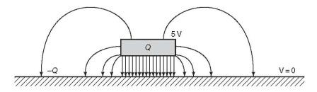
Figure 1. The electric field pattern of a circuit trace over a ground plane. (Source: Fast Circuit Boards – Energy Management)
More to Read
I have written a book titled Fast Circuit Boards – Energy Management, published by John Wiley and Sons. The basic physics behind transmission lines and board layout is covered in detail. There is some mathematics. There are many figures showing voltage waveforms that help explain wave action and radiation.
Buildings have walls and halls
Circuit Boards have traces and spaces
People travel in halls - not walls
Energy travels in spaces - not traces
Ralph Morrison has 50 years of experience in electronics engineering and is author of eight books, including Solving Interference Problems in Electronics, Grounding and Shielding Techniques in Instrumentation, and The Fields of Electronics: Understanding Electronics Using Basic Physics; This email address is being protected from spambots. You need JavaScript enabled to view it..


