 Optimizing multidomain integration in today's electronics.
The integration of field-programmable gate arrays (FPGAs) and printed circuit boards (PCBs) has emerged as a transformative approach to electronics systems design, giving rise to a powerful synergy that enhances performance, flexibility and efficiency. FPGA/PCB codesign, the art of seamlessly combining the capabilities of FPGAs and PCBs, has become a cornerstone in the development of cutting-edge electronics systems. This month, we'll explore the significance of FPGA/PCB codesign, its principles, benefits and the role it plays in shaping the future of electronics.
Understanding FPGAs and PCBs. Before delving into the intricacies of FPGA/PCB codesign, it's essential to grasp the fundamental concepts of FPGAs and PCBs and how they work together.
FPGAs are semiconductor devices that offer a unique advantage in terms of reconfigurability. Unlike application-specific integrated circuits (ASICs), FPGAs can be programmed and reprogrammed to perform a wide range of tasks. This flexibility in regard to component physical packaging and capacity of logic makes FPGAs ideal for prototyping, rapid development and applications where adaptability is crucial.
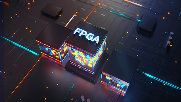
Figure 1. FPGAs may be repurposed for different tasks and applications, leading to a more cost-effective overall system design.
On the other hand, PCBs are the backbone of electronics systems, providing a physical platform for connecting and supporting various electronic components. The type of material used along with the arrangement of the PCB stackup, signal traces, power/ground planes, vias and components on a circuit board determines the functionality and performance of the final product.
Principles of FPGA/PCB codesign. FPGA/PCB codesign is a holistic approach that involves seamlessly integrating FPGAs into the PCB design process. The primary objective is to optimize the interaction between the programmable logic of FPGAs and the physical layout of the PCB. A tightly integrated multidomain and multidiscipline collaboration between the FPGA engineer and PCB designer is the goal. This integration is achieved by considering the following key principles:
- Communication and collaboration: Effective communication and collaboration between the PCB designer and the FPGA engineer is paramount. The PCB designer focuses on the design layout to include the FPGA, while the FPGA engineer works on the embedded software that will run on the FPGA. This collaborative effort ensures that both aspects are optimized for performance and functionality.
- System-level design: Rather than treat the FPGA and PCB as separate entities, adopt a system-level design approach. This involves considering the entire electronic system as a unified entity, addressing issues such as signal integrity, power distribution and thermal management at the system level.
- Partitioning and mapping: Enables optimization of FPGA pinouts so that connections are unraveled on the PCB. This reduces layer count/cost and improves performance. FPGA/PCB codesign involves partitioning the system functionality between the FPGA and PCB. Critical functions that benefit from the reconfigurability of FPGAs are implemented in the programmable logic, while other tasks are delegated to the fixed components on the PCB. This partitioning is crucial for achieving an optimal balance between flexibility and efficiency.
Benefits of FPGA/PCB codesign. Integration of FPGAs and PCBs offers a plethora of benefits that contribute to the overall improvement of electronics systems. Some key advantages include:
- Performance optimization: By leveraging the parallel processing capabilities of FPGAs, specific tasks can be offloaded from the main processor, significantly enhancing overall system performance. This is particularly beneficial for applications demanding high computational power, such as signal processing, image recognition and communication protocols.
- Flexibility and adaptability: FPGAs provide a level of flexibility unmatched by traditional fixed-function components. This adaptability enables quick iterations during the development phase and permits updates and modifications post-deployment, extending the lifespan of electronics systems.
- Reduced time-to-market: FPGA/PCB codesign facilitates a streamlined development process. The parallel development of hardware and software components permits faster prototyping and testing, ultimately reducing time-to-market. This agility is crucial in industries with rapidly changing requirements.
- Cost-efficiency: While FPGAs may have a higher upfront cost compared to fixed-function components, their versatility and reconfigurability often result in cost savings in the long run. The ability to repurpose FPGAs for different tasks and applications can lead to a more cost-effective overall system design.
- Enhanced system reliability: Integration of FPGAs and PCBs enables the implementation of redundant features and fault-tolerant mechanisms. This contributes to increased system reliability, making it suitable for critical applications where downtime is not an option.
Challenges and considerations. While FPGA/PCB codesign offers numerous advantages, it also comes with challenges and considerations:
- Complexity: Integrating FPGAs into PCB design introduces additional complexity. Coordinating the hardware and software design processes requires careful planning and collaboration among specialized teams.
- Power consumption: FPGAs can be power-hungry devices, and optimizing power consumption is a critical consideration. Balancing performance requirements with power constraints is essential for efficient system design.
- Cost of FPGAs: FPGAs can be more expensive than traditional fixed-function components. Careful consideration must be given to the cost-benefit analysis to justify the use of FPGAs in a given application.
- Security concerns: The reconfigurability of FPGAs permits enhancing the security of a product by reconfiguring when a vulnerability is detected. Ensuring the integrity and authenticity of FPGA configurations is crucial, especially in applications where security is a primary concern.
FPGA/PCB codesign represents a paradigm shift in electronics system development, offering a potent combination of flexibility, performance, and efficiency. As technology continues to advance, the demand for sophisticated and adaptable electronics systems will only increase. The synergy between FPGAs and PCBs, when harnessed effectively through codesign principles, empowers engineers to push the boundaries of what is achievable in diverse industries ranging from communications to healthcare and aerospace. Embracing FPGA/PCB codesign is not just a technological choice; it is a strategic decision to stay at the forefront of innovation in the dynamic world of electronics.
Stephen Chavez is a senior printed circuit engineer with three decades' experience. In his current role as a senior product marketing manager with Siemens EDA, his focus is on developing methodologies that assist customers in adopting a strategy for resilience and integrating the design-to-source Intelligence insights from Supplyframe into design for resilience. He is an IPC Certified Master Instructor Trainer (MIT) for PCB design, IPC CID+, and a Certified Printed Circuit Designer (CPCD). He is chairman of the Printed Circuit Engineering Association (PCEA); This email address is being protected from spambots. You need JavaScript enabled to view it..


