For boards headed for volume, plan your in-circuit test strategy up front.
The success of the manufacturing process is based on the execution and measurement of the health of each process step. Machines on assembly lines install thousands of parts every minute; therefore, throughout the assembly process, checks must be completed. Design-for-test (DfT) offers capability for testing, including component connectivity, electrical value, and proper component orientation. However, final testing – in-circuit testing capability – must be designed into the PCB at the layout stage.
Test engineers use test points to verify continuity and performance for every connection on the PCBA. This capability is a very powerful tool when looking for manufacturing defects on an assembly. While many tests can be run without required modifications to the PCB layout, ICT requires additional features for the PCB.
Types of test/inspection include:
- AXI post-wave inspection
- AXI solder joint inspection
- In-circuit testing
- AOI post-wave inspection
- AOI component measurement
- AOI solder joint inspection
- AOI solder paste
- Functional test
Should I include DfT for ICT? An engineering team must be in touch with several attributes of the PCB before deciding to add DfT for ICT. If the team can mark all the following “DfT required” checkboxes when making their analysis, the upfront expense might be considered an investment. Some basic reasons to justify DfT for ICT are:
- Provides probe access to nets on the PCBA that would not be accessible otherwise for testing and analyzing signal performance.
- In production volumes, tracking and measurement of the PCB processes are the keys to profitability.
- ICT can detect shorts, opens, lifted leads and missing parts.
- ICT can detect dead parts, wrong parts and bad parts.
- ICT can check for inverted polarity and missing socketed parts.

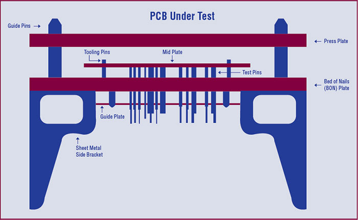
Figure 1. Tooling setup for a PCB under test.
Considering materials and time, PCBs that have ridden the conveyor far into the assembly process represent quite a bit of money. Checking for defects like those listed above with automated ICT at the completion of the assembly process confirms the quality of the assembly and, therefore, its value.
Catching and tracking defects during individual assembly processes helps show if there are any defects occurring consistently to any one part. For instance, if the same part is failing consistently on a run of PCBs, manufacturing engineers will perform a root cause analysis on the condition.
Incorporating DfT for ICT into a PCB layout can take time and add cost up front. Many ask, “Why do I have to pay for a test fixture whose only purpose is to check the quality of the EMS supplier? Isn’t quality their responsibility to check?” Yes, quality always falls to the EMS provider, no matter the run quantity. The true answer to the question is a matter of cost, however. Measuring quality on a run of 100 PCB assemblies will likely be accomplished manually. If it takes 30 minutes to test the PCB manually, the cost for testing the run is calculated at 50 hours at a rate of, say, $100 per hour, for a total cost of $5,000. That’s far less expensive than investing in a test fixture and implementing DfT for ICT. To apply a manual test strategy to 100,000 pieces, however, would take 50,000 technician hours, costing $5 million. Manual testing such a large run of assemblies is not feasible. This exaggerated example is the reason to pay for automation. DfT for ICT reduces testing time to seconds and therefore saves overall cost, even after investing in test equipment.
Test points. Test points are etched target shapes which include short routes making electrical connection to the circuit nets of the PCBA. They are typically round, 0.035" (0.89mm) or larger, and clear of any solder resist or legend ink that would impede electrical connectivity when in contact with a test probe. Test points can be added to the schematic and even include reference designation, if required. In many cases, if testability is called for at the beginning of a layout project, the EE will work to address the requirements into the layout at the time of placement, prior to routing.
Test point spacing. Spacing the test points sufficiently is paramount to good DfT. Test point spacing of 0.100" (2.54mm) is considered good by test engineering stakeholders because such spacing permits use of least expensive test probes and ideal ease of access. However, real-world design density will not always permit such robust spacing. In this case, reducing grid spacing by 0.025" (0.64) – to 0.100", 0.075", or 0.050" – is considered acceptable, though the smaller spacing will yield a higher cost fixture.
Test strategy and requirements. A test point strategy is usually determined at the time of parts placement. It’s important for it to be clearly developed to identify goals, cost, quality and scheduling. Be clear regarding which nets need to be accessed, whether this is through a note or by adding test points to the schematic.
The general requirements for adding test points to a PCB layout are simple: test points are ideally added to the non-component side of a PCB. However, if the side selected for test points includes components, avoid placement near parts taller than 0.200" (5.08mm). Common test point shape and size is circular, with an ideal diameter of 0.040" (1.00mm). This diameter ensures spring-loaded test point probes will be placed accurately enough to raise the probability of contact to the test pads to 100% per 1,000 hits. If space is limited on the layout, test point size may be reduced slightly, to 0.035" (0.89mm). Further reducing the diameter will increase the probability of a probe miss significantly, however. Generally, adding a single test point per net on the PCBA design, if possible, makes the test engineering stakeholders happy. Also, it helps if many extra test points can be added to ground and power across the PCB for ease of access.
When implementing DfT for ICT, once the PCB is manufactured and a test fixture is built, future changes to the PCB should not disturb previously placed test points. It is recommended they be locked down in the design. While it is easy to move a test point on a layout, it is very difficult and expensive to retool a test fixture to match the change.
The Surface Mount Technology Association (SMTA) has published TP-101E, Testability Guidelines. This comprehensive guide is a great go-to that should be read by all project stakeholders to better understand their test engineering counterparts. This should interest PCB designers because the publication lists several general guidelines for creating test equipment for the designed board. In addition, the guide describes 32 probing-fixture guidelines the test engineer must adhere to.
JTAG. With high-density requirements on PCBs continuing to rise, having real estate to add test points for 100% testability on a PCBA is a rarity. Implementing partial test point coverage can make some test engineers cringe and ask, “If you’re not fully testing, why test at all?” Missing test points on a PCBA with no physical space remaining is a weak compromise. However, there is another option.
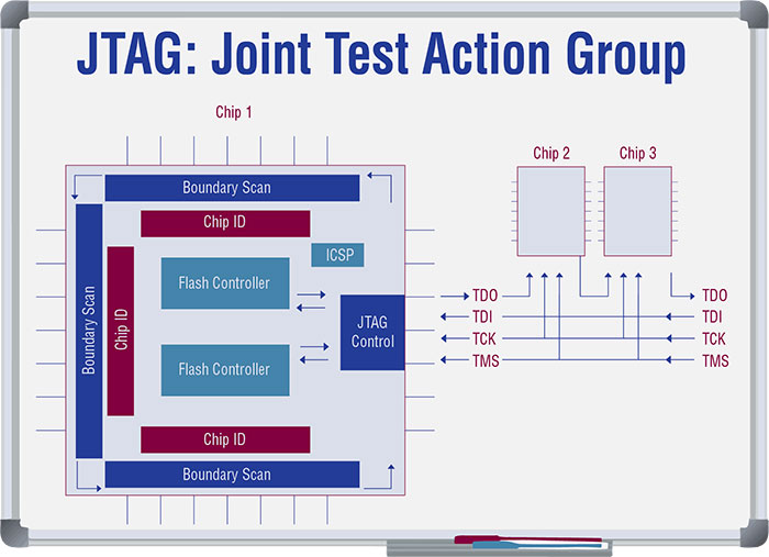
JTAG, the Joint Action Test Group, was formed by a group of companies in the 1980s to define extra silicon added to the workhorse chips on a board. This extra silicon would then permit devices to be put into a “test mode,” giving users control of the pins on the device. It is very similar to boundary scan, another common test protocol. Both are governed by IEEE 1149.1-6. The JTAG test spec defines the signals to be accessed (FIGURE 2). A PCB design engineer needs to be aware there is a minimum of four wires. The signals used are:
- TCK (test clock). This signal synchronizes internal state machine operations.
- TMS (test mode select). This signal is sampled at the rising edge of TCK to determine the next state.
- TDI (test data in). This signal represents the data shifted into the device’s test or programming logic. It is sampled at the rising edge of TCK when the internal state machine is in the correct state.
- TDO (test data out). This signal represents the data shifted out of the device’s test or programming logic and is valid on the falling edge of TCK when the internal state machine is in the correct state.

Figure 2. JTAG specification testing schematic.
An optional signal, TRST (test reset), when available, can reset the TAP controller’s state machine.
Conclusion
When is the best time for considering DfT? Simply put, test engineers are important stakeholders in any PCB design project that will be going to volume. As circuit performance requirements are defined, questions about how performance will be tested and verified do not naturally come to mind for other project stakeholders. Test engineers must be provided schematics and brought to the table at the beginning of a project to address whether testing is required, what equipment will be used, and provide estimates for initial cost.
Once the decision is made that testing will be required on the PCB, DfT can be implemented during the layout phase of the PCB. The design database can be set up to audit each net for testability. The software should be able to export a DfT report showing all net names with respective test point x-y locations, which can be of great use to the test engineer when creating a fixture. This design-for-test practice ensures the best chance for all testing requirements to be successfully included in the design.
This excerpt of The Hitchhiker's Guide to PCB Design was written by EMA Design Automation, with special contribution from David Ruff. Download to learn more about PCB design stakeholders and real-world, actionable PCB design tips from industry experts (go.ema-eda.com/pcbguide).


