
Part two of how to design a flex circuit.
Ed.: The first part of this series was published in March 2014.
Flex PCB routing shares many of design rules as rigid PCB routing, with a few extra rules that apply specifically to areas of the circuit that will be flexing. The “extra” rules are:
- Keep plated vias out of flexing areas. When a circuit is bent, there will be stretching and compressing forces that come into play that can wreak havoc on plated vias. Put ’em somewhere else!
- Conductors should be routed through flexing areas perpendicular to the bend. For a single flex to install this is not especially critical, but if the flex will be subjected to multiple flexing cycles during its service life, this becomes a concern.
- Avoid directional changes in flexing areas. If the preceding rule is followed there won’t be an issue with this. Again, this is not critical in a flex-to-install application, but it is if there will be more than a few flexing operations. If direction changes absolutely cannot be avoided, use an arc rather than a sharp corner. The larger the radius of the arc, the better.
- Avoid changes in conductor width in flexing areas. Conductor width changes can create stress concentration points that may ultimately lead to conductor cracks.
- Apply fillets to all pads, including vias and pads that will be soldered (Figure 1). Flexible substrates are much more fragile than rigid substrates, leaving copper traces more prone to damage at stress concentration points. The point where a small conductor connects to a pad can be a stress concentration point. A fillet at this junction will eliminate this issue. In my 30-plus years of flex circuit design, I cannot point to a single application where a pad fillet caused a failure, but I can point to dozens of occasions where the lack of pad fillet did cause a failure. Pad fillets don’t cost a nickel, so there is no reason not to use them.
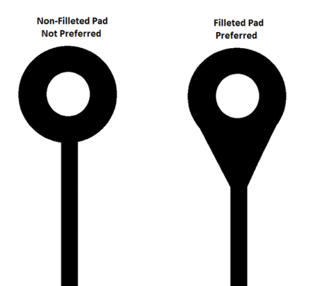
Figure 1. The pad on the left is not filleted, which makes the point where the conductor meets the pad a potential failure point. The pad on the right is filleted, eliminating this potential failure.
- For very small conductors (less than 5 mils), keep them on internal layers. This will provide the advantage of keeping plated copper off them (more on this topic to follow), and will also move them closer to the neutral bend axis to reduce stress when the circuit is flexed.
Stress concentration points. I cannot overstress (no pun intended) the importance of reviewing the design for stress concentration features in flexing zones. The construction of the circuit and conductor features should remain constant and unchanged in and around an area that will be bent. The vast majority of flex circuit failures I have seen were caused by features that elevated mechanical stresses in a small focused area or point. Many things can cause this; here are some of the most common to keep out of a bending or flexing area.
- Openings in cover or solder mask. These openings and the conductors exposed by them are prime candidates for damage if they fall into an area that will be flexed.
- Any change in overall circuit thickness. The rigidity of the part will change with any change in circuit thickness, which can focus stress in the thinner (and probably most fragile) area.
- Copper plating on outer conductors. Any application that will see a moderate (a few hundred) to high (thousands) number of flexing cycles should utilize rolled annealed (RA) base copper rather than electrodeposited (ED) copper. The annealing process makes RA copper the most resilient in flexing applications. Unfortunately, copper plating the conductor surface will negate any benefit gained by the annealing. Plated copper will crack much sooner than the RA copper it is plated to and will take the RA copper with it. Pads-only (button) plating will not cure this because most vendors’ process for POP requires a thin-plated copper flash over the entire panel prior to plating the pad areas. On low-layer-count flex circuits there may not be a choice, but on multilayers flexing conductors should be positioned on internal non-plated layers.
- Other surface plating on conductors (especially nickel). Nickel plating is brittle and should be kept well away from bending areas. Other platings can increase rigidity due to the increased thickness, which in turn can create stress concentration points.
Once again, your flex circuit manufacturer may not be able to tell you everything that will work, but I can guarantee that they will know what does not work (those experiences are hard to forget). Believe me, they want your design to work as much as you do.
Mark Finstad is a senior application engineer at Flexible Circuit Technologies (flexiblecircuit.com); This email address is being protected from spambots. You need JavaScript enabled to view it.. He and co-“Flexpert” Mark Verbrugge from PICA Manufacturing Solutions (This email address is being protected from spambots. You need JavaScript enabled to view it.) welcome your questions.


