 The outline of a PCB can serve as more than a simple perimeter.
The perimeter of a PCB defines the extent of whatever electronics have to be packaged therein. The outline can also serve other functions.
Printed circuit boards come in many shapes and sizes. The first thing the outline gives us is the resulting routable area. The positional variation of each layer in the stackup requires us to compensate with a little pullback of the metal from the edge.
These days, pulling the metal back from the edge by 8 mils (0.2mm) is sufficient for most fabricators. I went to a PCB conference walking from booth to booth and asked all the fabricators what their minimum pull back from the edge would be for production quantities. A few of them, call it 20%, said they could plate the board to within 5 mils (0.127mm) of the edge. In a special case, we used lasers to define the edge and had metal just 2 mils (0.05mm) away.
The next increment is to plate right to the edge and wrap copper around to the other side. Edge plating is used in cases where we want to create a more complete Faraday cage around a circuit. It’s also possible to pass voltage and ground from the top to the bottom around the edge of the board or even using a slot within the outline of a board.
All you have to do is draw your shape(s) right up to the edge on both sides and specify that those locations have the metal wrapping around. A few unrelated teams have asked for this technology, so it’s not that rare. In addition to stemming EMI emissions, the metal also prevents the innerlayers from absorbing moisture through the edges of the board.
The edge of the circuit board becomes the connector. Goldfinger is more than just a James Bond movie. A row or rows of gold fingers can take the place of a connector. One common application is the PCIe connector. In this instance, the gold fingers are plated on both sides of the PCB. Consequently, the board must use a standard PCB thickness of 0.62" (1.6mm) so that the fingers on both sides properly engage with the receptacle.
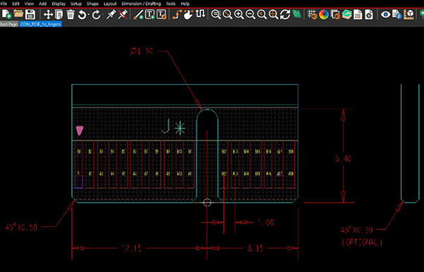
Figure 1. A PCIe connector is a common interface that makes use of the board edge as half of the pairing with what amounts to a printed connector. A few pins are pulled back from the edges so that the other connections are made first and disconnected last.
Using the edge of the board as a connector is the norm for flex circuits, many of which are little more than bespoke cables between rigid boards. What is known as a zero-insertion force or ZIF connector expands on the finger idea with an additional row of contacts and a companion connector that has a latch that locks the ZIF tail in place.
While I created the PCIe connector footprint by hand, the ZIF connector geometry is too convoluted for me to want to try. The connector vendors know this and provide the interlocking pad geometry in the popular ECAD formats.
Figure 2. A PCIe mini edge card connector. The PCB thickness is standardized on 0.8mm, requiring its own class of fine-pitch connectors.
Edge connectors for HDMI are simpler in geometry but the thing I remember when these came out is that the spec calls for more durable gold on the typical edge connector. The pass/fail criteria are 10,000 insertion/extraction cycles. That meant that you needed hard gold instead of medium, which is a selective plating step just for the edge connector.
The selective gold plating requires the fingers extend to the very edge of the PCB. The cost and pushback from the fabricator usually mean we forgo this process unless absolutely necessary. Note the spec for USB dongles is 5,000 times in and out of the connector. That seems more likely to actually happen than with the HDMI use case.
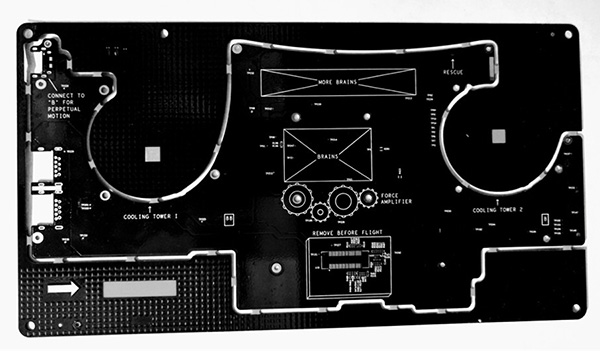
Figure 3. Dual fans and numerous connectors define the outline of this main logic board. Whimsical silk screen to distinguish each prototype optional.
Speaking of USB, implementing those connectors in a low headroom environment like a phone, tablet or laptop often finds us using a mid-mount connector. The feature here is that a cutout in the edge of the board is taken up by the connector body. Connector vendors like some tight tolerances, sometimes describing a cutout feature as a minimum or a maximum value.
In the past, I would have made sure these offbeat dimensions were not forgotten. I’d put the key dimension on a layer that shows up as part of the fabrication drawing. Then what happens is that the vendor gets confused and wants a nominal dimension with a bilateral tolerance. I try to look ahead to anticipate the vendor’s reaction. None of them seems to want a unilateral or limit tolerance giving an upper and lower bound.
A technique for ensuring stackup layer order. Many printed circuit boards are for development purposes and have some extra real estate not found on the production form factor. That open area on the big board can be used to put the number 1 on the top layer followed by a 2 on the next layer and so on through the board in sequence. Clearing out the copper above and below these numbers lets us confirm that the stackup is laminated in the correct order.
But what can we do when space is at a premium? This is a situation where we can violate the route keep-in with a little tab on the top layer that juts out to the edge of the board. Below and to the right would be a tab on the next layer down and cascading down a stair-step pattern to the bottom layer. The whole thing takes place in between the keep-in area and the edge of the board. It is a rule violation, and we keep those tabs separate from each other in the lateral direction so that nothing shorts out in the z-axis. The tabs are usually part of the ground but could be floating if there is nothing to join.
John Burkhert Jr. is a career PCB designer experienced in military, telecom, consumer hardware and, lately, the automotive industry. Originally, he was an RF specialist but is compelled to flip the bit now and then to fill the need for high-speed digital design. He enjoys playing bass and racing bikes when he’s not writing about or performing PCB layout. His column is produced by Cadence Design Systems and runs monthly.


