 Put the pedal to the metal in your PCB layouts.
Printed circuit board design evolves over time and the rate of the evolution is not slowing. High-speed digital design becomes a key topic as we move forward.
By the time you read this, I’ll be officially old. Early retirement age is 62 and I was born in ’62 so I’m eligible for those senior discounts. One of the things that happens as we age is time seems to go by even faster. We’ve seen so much, less is novel. We’re not plowing new furrows but rather deepening ones we’ve tracked before.
I say that to say this: Circuits keep switching faster all the time. What worked in my early days no longer gets it done. My first computer didn’t have a hard drive. It had two floppy disk drives, and they were the ones with 360KB rather than the smaller, stiffer 1.4MB. I had DOS on one floppy and a modem driver on the other. The baud rate was a blazing 1,200B.
Now, look at the solid-state thumb drive on my keychain or the SD card inside my action camera. We’re talking up to 2GB for SD cards. It doesn’t end there. SD has morphed to SDHC to reach the “high capacity” of 32GB. Then, we move up to SDXC where the extreme capacity goes to 2TB. We’re not done. SDUC packs a whopping 128TB. All these form factors also come as micro SD cards to shrink things further. Think we’re done? I doubt it.
Now, take 128 billion and divide by 360,000. That's an improvement of over 350,000 times what I started with on my Zenith Z171 “luggable” machine from the late 1980s. The potential storage is orders of magnitude beyond the ancient equipment while consuming a tiny fraction of the physical space of a floppy drive.
Reading that much data on the old gear would most likely still be in process all these decades later. That’s a long timeline but it illustrates what we face in today’s printed circuit board layouts. The exponential expansion of memory is met by processing pipelines that drive the intense applications found in mixed reality, robotics and other leading-edge hardware.
High-speed transmission techniques. Low voltage differential signaling (LVDS) is the cheat code to get more done with less power consumption. While very popular in mobile applications, the same efficiency is important in the data centers as well. From a board geometry standpoint, this is basically the same as the usual differential pair routing. Note that TTL requires 5V swings, while CMOS runs on 3.3V.
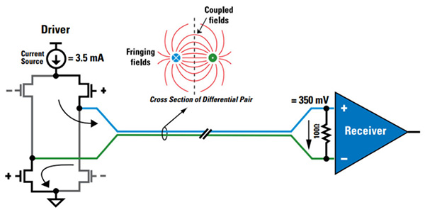
LVDS incorporates smaller current swings which means that they make better neighbors in a crowded design. (Source: Texas Instruments)
The same benefits from typical differential pair routing include lowered EMI, rejection of external interference and higher data rates over single-ended transmission lines. Meanwhile, the voltage requirements for LVDS are capped at 450mV with a floor of 250mV, an order of magnitude lower than TTL/CMOS voltage requirements.
The data rate skyrockets in this scenario. Part of the system may be on the older tech, so it’s common to use serializers to combine numerous streams on the LVDS pair and deserializers to expand the LVDS signal back out to SATA, HDMI or other interfaces that use more wires for the same data rate. The same type of SerDes is used between fiber optic cables and copper traces on the network PC boards. Modern SOCs make use of dozens of cores while the GPUs have equivalent throughput but are marketed differently in order to boast even higher numbers. We have some work to do.
Thirteen tips. My well-earned advice for good high-speed layouts:
- Like any board, starting with good fundamental power integrity will solve many of the coexistence issues before they crop up.
- Placement supporting short line lengths while segregating components by power domain will help create an efficient routing result.
- Isolate noise sources such as crystals and other clocks with additional space and/or guard bands. That process helps keep the intersymbol coupling to a minimum.
- Short traces on top, longer ones on innerlayers. We don’t want to use vias in general, but they are the lesser of two issues when it comes to electromagnetic interference on longer runs.
- Use two ground vias placed in symmetry with the differential vias. If no room is available for ideal ground via placement, then use more-than-minimum spacing between the signal vias and asymmetric ground via(s). Basically, don’t cozy up to one signal via if you can’t do the same with the other.
- Not just via symmetry, the gathers from the pins and vias ought to form a Y with equal spread.
- Do I even have to ask you not to cross over a gap in the reference plane?
- The gap between via and trace should be a bit more than the gap from via to supporting plane layer(s) to permit misregistration.
- Avoid routing near the edges of the board if possible.
- Phase matching between the positive and negative elements of the pair should be addressed with an appropriate jog in the shorter trace so that the two lines are in sync before any length matching. If the two lines of a pair are a different length, you have less to work with for overall length matching.
- Dynamic phase matching is where that effort takes place on any bend. The idea is to keep the two waveforms in lock step for the entire flight. That’s where the inherent isolation really shines.
- Receive chains are typically more susceptible to EMI than transmit chains. Give them priority in terms of isolation.
- Use simulation in order to find and fix any unexpected issues. Everything done on the layout is a trade-off. Prototypes are still required but this cuts down on the number of cycles it takes to create a conforming design.
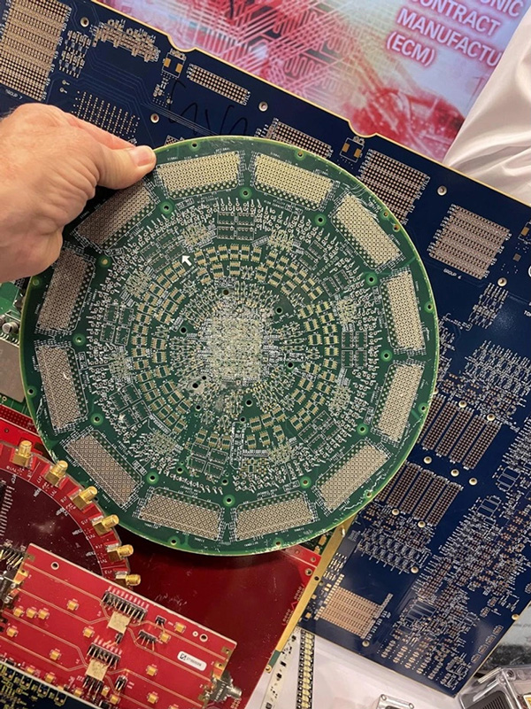
Known as probe cards, these are some challenging designs. They are typically circular to give us a chance of getting all the signals from chip to perimeter with proper length matching. (Source: Author)
Hardware is the scaffold that supports the software. The software, meanwhile, is rapidly expanding its reach into many aspects of our lives. Somewhere down the road, we may move into units of measure even smaller than a nanometer to create new silicon. We have to keep up with those chips and manage all that energy density with new solutions. Materials and processes evolve, and our board designs are the link in between all of this progress.
John Burkhert Jr. is a career PCB designer experienced in military, telecom, consumer hardware and, lately, the automotive industry. Originally, he was an RF specialist but is compelled to flip the bit now and then to fill the need for high-speed digital design. He enjoys playing bass and racing bikes when he’s not writing about or performing PCB layout. His column is produced by Cadence Design Systems and runs monthly.


