Why a tooling hole remains the answer for an end-to-end process.
Technology marches on and the result is a decreased margin for error. Even the language must adapt as mils give way to microns, because one thousandth of an inch is too coarse a measure for modern PCB geometry. As traces and spaces shrink to accommodate the latest chips, the onus is on fabricators and assemblers to achieve greater precision in all aspects of manufacturing.
Where does it end? Could Intel's new 2nm fab be the last stop? It seems so but I would not bet on it. Somewhere, somebody is working on angstrom class devices. Why not? Well, a single atom of copper comes in around 0.23nm, so Intel is depositing about eight or nine atoms of copper across the width of a connection. To quote Carl Sagan, “Billions and billions,” but we’re scaling down rather than up.
Gains made in foundries carry over to the printed circuit board. Thus, we must get better with each generation. Etch processes give way to additive processes to get down to the 25µm lines/spaces realm. That might be enough, for now.
Meanwhile, the PCB stackup must accommodate the increased circuit density one way or another; more traces per layer or more layers overall. Either way, the precision of layer-to-layer alignment is tightening on a regular basis. We’re likely to see a greater use of lasers and other means, such as MSAP, to get reliable results at this scale.
The best alignment method for PCB fabrication remains the humble tooling hole. This is a set of non-plated holes with precisely defined locations and even more precise diameter tolerances. They are always non-plated because the plating process is too imprecise for repeatable fixturing. These holes key the board or panel to a matching set of pins on a fixture or, I should say, fixtures.
These precision holes in the bare board align the layers during initial lamination and any subsequent lamination cycles. After the press, the board is placed in another jig for application of solder mask and silkscreen. Yet another fixture will use them for electrical probing to find opens and shorts. Good panels will then be put on a robotic assembly line and then on to a soldering machine using the same holes. Some additional testing and automatic optical inspection (AOI) may follow.
Given all those uses, it is advisable to have the tooling holes in an arrangement that precludes the possibility of putting the board on backwards or upside down. Normally, we want three of them, to ensure only one way to load the board into each fixture. If four holes are used, you want them asymmetric (FIGURE 1). Regardless of the quantity, they should be pushed toward the corners (if there are corners) to make it easy to align the pins and holes each time. On-board tooling holes may get a second life as mounting holes if you’re not counting on the hardware for a thermal path.

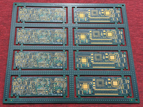
Figure 1. While there are four tooling holes, the panel is not an exact square. It must be flipped to complete the assembly. The same paste stencil and x-y data apply no matter which side is up. There are two ways to put this panel on the mating fixture and both are used for what is known as an A-B flip panel.
Back in the good old days, tooling holes came in one size, 125 mils, with a plus/minus tolerance of one mil. Now, there is an 89 mil hole too, because everything in this game shrinks over time. Unilateral tolerances are often applied where the pin will be the nominal value with a plus tolerance but no negative tolerance. The hole then gets zero oversize and a small negative tolerance. The actual numbers come down to what the fab shop can do on a best-effort basis. It’s almost an interference fit but not quite.
Smaller boards found in a smartwatch or similar device do not have room for tooling holes on the board, so the holes become a standard part of the assembly sub-panel. The sub-panel is maintained through fab, assembly and test and only broken down once the boards are known to be working to the standard requirements.
Now we’re set up for component placement on the assembly line. No, we aren’t. The pick-and- place machine has a camera that can find a specific set of features on the board. These features are called fiducial marks, and they help the robotic arm calibrate on the exact location of the components.
A typical board-level fiducial mark, or fid, will consist of a 1mm dot of exposed copper surrounded by a 3mm clearance in the solder mask and other circuit patterns. A solid plane on the layer below the fid is important so the camera can recognize and register on the dot without the distraction of a circuit pattern underneath. No drilling is involved, although to the uninitiated it may look like a hole location.
Fiducials can also come in a smaller size for use as a local fiducial. These are placed just outside of the footprint of any fine-pitch components so the optics can zero in on a more precise location than if it were calibrating over the entire board area. It’s advisable to address these early in the design, perhaps even incorporating them with the actual footprint of the fine-pitch/high pin-count devices.

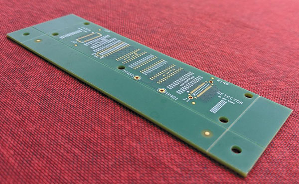
Figure 2. The remains of a break-off panel using V-scores. Larger fiducials on the tabs and smaller ones locating the fine-pitch connectors on the actual board.
In addition to circles, I’ve seen squares and crosses used as fiducial marks. I do not recommend them simply because the etch process isn’t that good at creating 90° corners, especially inside corners. With etch-defined circuits, a tiny cross comes out looking more like a blob than what is on the artwork. These are more common on device packages where the metal is sputtered onto the substrate. They still come out looking somewhat organic.
Between tooling holes and fiducial marks on the panel or board, we can control placement to the degree the components self-center during reflow soldering. This works best when the pads are identical to one another. Trace width and launch direction play a role in how the capillary action pulls the part to the middle ground while the solder is in its liquid state. Flooding copper over one pin and not the other(s) will undo all that effort.
You could shrink the solder mask of the flooded pad(s) so that it becomes the same size as the non-solder mask defined pads. That mitigates the problem but is not as effective as a fully symmetric design. We look to thermal spokes as a means of evening the thermal load on each pin. Many assembly defects arise from imbalanced solder joints. A perfect placement can be undone by inattention to this detail.
Things will go wrong now and then. The goal is to minimize the number of rejected boards. By the time they are in assembly, we don’t have many options other than playing with the solder paste stencil and thermal profile of the soldering machines. It is up to us to keep the process window wide open so fabrication and assembly become boring. That’s the best kind of process right there. •
John Burkhert Jr. is a career PCB designer experienced in military, telecom, consumer hardware and, lately, the automotive industry. Originally, he was an RF specialist but is compelled to flip the bit now and then to fill the need for high-speed digital design. He enjoys playing bass and racing bikes when he’s not writing about or performing PCB layout. His column is produced by Cadence Design Systems and runs monthly.
PCB West: The leading technical conference and exhibition for electronics engineers. Coming Oct. 4-7 to the Santa Clara (CA) Convention Center. pcbwest.com
