Does changing the clock make any difference to the PCB layout?
Every six months, it becomes apparent not enough of my household items are part of the “Internet of Things.” (Cue ominous violin squeals.) Can we talk about my spouse’s wall-clock fetish? At least the one in the bedroom doesn’t tick! And, of course, if a battery is near its end, an adjustment will probably put it out of business for good. It’s always something getting me back up on that step ladder.
Setting and resetting clocks is also a thing in PCB design.

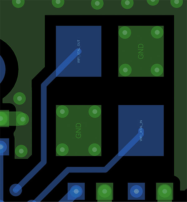
Figure 1. The ground pour (green) surrounds the crystal but does not engage with the ground pins. The ground plane on layer 2 is similarly slotted around the crystal to help contain spurious emissions.
Keep the working circuits intact. The engineers on the analog side of the coin get very attached to a circuit that works. If something is working with sufficient margin, then don’t even get near it with “arbitrary and capricious” revisions. Tread lightly in those situations, as there are many ways for things to go haywire. Consider the crystal as a hostile device from the start. That way, if it must grow, the other geometry already leans away from the danger zone.
The main source of frustration during RF chip/board bring-up is out-of-band emissions. Some odd-order harmonic can end up exceeding the mask. There will be an unwanted spike or lump in the graph. Bandpass filters have their limits and cost money while using power. The analog engineers spend nights and weekends passionate to solve these issues. They thrive on tweaking circuits and taking measurements.
A subtle tuning stub or an inductive neck-down on the power feed can be all it takes to solve the issue, but now you’ve changed the little world around you, and anything can happen. Radio frequencies are everywhere to be picked up and propagated. Making one strong sine wave without disturbing the spectrum in other ways is a tough assignment. We have good reason to venerate a fully compliant link in the chain.

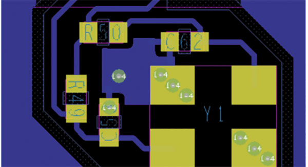
Figure 2. It would have been cleaner to rotate Y1 and align the passive elements. We compromised to fit inside the EMI shield.
External oscillators: an alarming clock. The cautionary tale is digital circuits above a certain data rate will start to resemble analog circuits. Most MCUs have an option for an external oscillator. What is that? It’s usually a way to override the system clock and impose a different cycle time on the system. Why do so? In general, overclocking increases performance, while underclocking saves power. Some are for bootup. Others are only active when certain functions are in use. When it’s on, the string on ones and zeros is nonstop clatter to the rest of the circuitry.
The net-names associated with these clocks will typically include the letters “XO.” Popular frequencies for these crystals are in the kilohertz range. Each of those available frequencies will have its own harmonics – and its own package size!
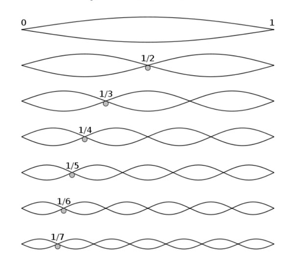
So, maybe you start at 16KHz as the external clock. That’s in the upper audible range, but, of course, the vibration of the crystal is imperceptible without measuring equipment. Still, byproducts of 16KHz include 32KHz, 48K, 64K, 80K, 96K, 1.12MHz and so on.

Figure 3. A fundamental frequency shows sympathetic wavelengths often generated along with the original. (Source: SoundGuys).
Keep the crystal circuit short and free of vias. It’s mostly on every other node, but there are many intersections where 16KHz has common multiples with other frequencies found in nature. A strong resonance will be a detriment to the circuit, particularly when it comes to coexistence. A compact XO circuit is a must, but you can’t always get what you want.
One of the worst scenarios is when XO pins are located deep inside the rings of pins of a BGA. Usually this is found in a small enclosure where there isn’t sufficient space on the bottom of the PCB for tall components. This means the XO traces will be longer than usual. A typical example is the power management integrated circuit (PMIC) in which all the peri-meter pins seem to be voltage in or out.
The crystal might be on the opposite side of the board but just as likely off in a corner on the side of the board that has the headroom. Make it the corner away from the receive chain. The TX side isn’t great either but is usually less of a victim than the RX side, if it’s one or the other. Look for a neutral corner with the least amount of signal traffic.

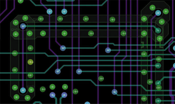
Figure 4. The vertical trace on the left (magenta) and the horizontal continuation (cyan) show how to create a guard-band around particularly noisy connections used by externally clocked devices.
Routing the external oscillator lines out from under a device should be done first. If you have any freedom in the fan-out, a wide path should be carved out for these traces. There’s always one row on a BGA where vias can fan in different directions. That row is often around the center line, but it doesn’t have to be.
Other signals in the region should go on other layers, allocating as much extra space as possible to the clock nets. If you can create a guard band around the noisiest signals, then you can call it good. We always want an optimal placement that allows no-brainer routing. Because we can’t always get what we want, we do what we must to get by.
John Burkhert Jr. is a career PCB designer experienced in military, telecom, consumer hardware and, lately, the automotive industry. Originally, he was an RF specialist but is compelled to flip the bit now and then to fill the need for high-speed digital design. He enjoys playing bass and racing bikes when he's not writing about or performing PCB layout. His column is produced by Cadence Design Systems and runs monthly.


