
The basics of line impedance influences.
Impedance and impedance are especially important with high-speed design when related to signal integrity. In this, the first of a two-part column, we’ll go back to the basics of impedance/impedance control and consider what influences line impedance. In part two, we’ll set about controlling it.
To ensure proper signal integrity for a PCB that incorporates high-speed digital devices, it is essential to control the transmission line impedance.
So, what do I mean by “proper signal integrity?” I refer to signal quality/purity that at the end helps meet the timing requirements of high-speed digital devices.
Increasingly, circuitry features signals with ultra-fast switching times, which must comply with ever-tightening design-constraints like skew matching or setup and hold requirements.
One of the basic constraints – the “mother” of all high-speed constraints, if you will – is line impedance, be it single-ended or differential (Zdiff). Where high-speed digital ICs are concerned, the OEM or standard/protocol will specify the required impedance. FIGURE 1 shows some examples.
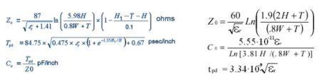
Figure 1. Two sample formulas to compute a single-ended impedance.
Alternatively, calculate the desired line impedances yourself. For this, a number of formulas (FIGURE 2), with varying degrees of accuracy.

Figure 2. Equivalent circuit of a transmission line modeled as a cascade of lumped elements.
Common to all is they marry your design elements (e.g., trace lengths and widths, layer stacks, etc.) with the physical properties of the intended manufacturing process (predominantly the materials being used). Such formulas can yield accurate results, especially for single-ended structures, but are not suitable for coupled situations (like differential pairs). Here, more advanced techniques like field-solvers are required.
For many PCB designers, dealing with impedance is their first and sometimes only contact with the complex world of high-speed design.
Transmission Line Impedance
The electrical behavior of a signal line is, in principle, dictated by conductor geometry. Once you know the material constants of the surrounding media, you can calculate the dielectric constant, εr, which gives the electrical parameters of a line. The trace width, together with the height of the trace, determines the geometry of the trace.
Every electrical conductor comprises capacitance, inductance, and a frequency-dependent ohmic resistance. (See Figure 1 showing a common electrical equivalent circuit of a transmission line segment.) With increasing frequencies, the parasitics and transmission line impedance cannot be ignored, or they will influence and may distort the signal. As a consequence, the signal becomes an active interconnect instead of a passive connection.
A change in the conductor width always means a change to the cross-sectional area, having an impact on the maximum current and thermal behavior. In applications where very high clock speeds or data rates, and relatively long electrical line lengths, are required (e.g., backplanes), ohmic resistance can also play an important role.
However, the occurrence of a change in the electrical behavior of a conductor through varying its height is relatively rare. Typical multilayer stack-ups use conductor heights of 17μm to 36μm. These are mainly determined by mechanical constraints such as the overall board thickness. It should be mentioned the manufacturing process will deform the ideal rectangular (cross-sectional) shape of the trace (etching effect).
Back to Basics
The characteristic impedance or surge impedance (usually written Z0) of a uniform transmission line is the ratio of the amplitudes of voltage and current of a single wave propagating along the line: that is, a wave traveling in one direction in the absence of reflections in the other direction. Characteristic impedance is determined by the geometry and materials of the transmission line and, for a uniform line, is not dependent on its length.
The standard unit (SI unit) of characteristic impedance is ohm (W). The characteristic impedance of a lossless transmission line is purely reactive, with no real component. Energy supplied by a source at one end of such a line is transmitted through the line without being dissipated in the line itself. A transmission line of finite length (lossless or lossy) terminated at one end with an impedance equal to the characteristic impedance appears to the source like an infinitely long transmission line and produces no reflections.
What does that mean for a PCB designer in terms of signal integrity?
It can be shown that an equivalent definition of characteristic impedance is as follows: the characteristic impedance of a line is that impedance which, when terminating an arbitrary length of the line at its output, will produce an input impedance equal to the characteristic impedance. This is so because there is no reflection on a line terminated in its own characteristic impedance (per the Wikipedia definition).
The characteristic impedance of a transmission line is determined by the following factors:
- The trace geometry (trace width and height);
- The distance between the signal layer and the current return path; and
- Dielectric constant, Σr.
To achieve the desired impedance and to match the required tolerances, PCB designers tend to work closely with the PCB manufacturer.
Based on the favored stack-up and the PCB layout demands, a proper impedance calculation method should be chosen. Guesswork and hope are not good engineering practices here, and the impedance targets for at least all critical signals must be determined before routing begins.
In today’s PCB manufacturing processes, tolerances of 5 to 10% for impedance values can be achieved with appropriate material selection, proper design of the layer stack structure (FIGURE 3), trace geometry planning (including any influence the etching process may have), and careful layout.

Figure 3. Impedance-controlled stack-up within a PCB tool.
Table 1. Example Impedance Constraints and Tolerances for Various Technical Protocols (Mostly Differential)

Ralf Bruening is product manager/senior consultant high-speed design solutions at Zuken (zuken.com); This email address is being protected from spambots. You need JavaScript enabled to view it.. He will speak at PCB West in September at the Santa Clara (CA) Convention Center.


